Summary
This blog continues from part 3 of the supply voltage interruption tester (unit) post.
Covered in this blog are aspects of the Printed Circuit Board (PCB) implementation for the Infineon (Cypress) CapSense and output driver temperature measurements.
CapSense
CapSense has been available for over a decade however, I had not had a practical use for this technology on either a hobby or professional level until the interruption tester design.
For the interruption tester, CapSense buttons were chosen instead of standard mechanical push buttons. During testing of the prototype interruption tester, daily variations in Capsense measurements were noted. While the variation resulted in sensitivity changes, tuning the CapSense component addressed most issues.
For the PCB layout, loosely following the CapSense PCB guidelines (Section 6.4) on a two-layer PCB resulted in poor performance. Tuning out interference or crosstalk was not achievable. This was likely due to the trace-to-trace spacing although the root cause was not investigated.
 |
| CapSense Trace-to-Trace Spacing - Courtesy Infineon |
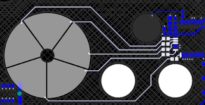
The design used in this blog uses a four-layer PCB with increased spacing between CapSense traces. For the 0.2 mm CapSense traces on the bottom layer, a 1.2 mm trace separation was used where practicable. Cross-channel triggering on CapSense lines no longer occured.
 |
| Interruption Tester - Radial Slider Trace-to-Trace Distance |
Highlighted in the image below are the Capsense traces leading to the microcontroller for the radial slider.
 |
| Interruption Tester - Trace-to-Trace Spacing for Radial Slider |
Output Driver Temperature Testing
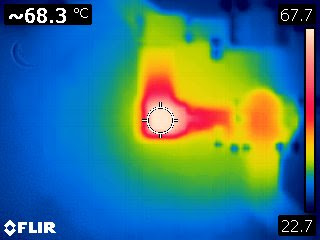
For tests 1 to 3, the high-side drivers (IPS160H) were driven into a resistive load to create a load of approximately 2.4 A. Temperature measurements were taken of the high-side driver(s) active for that test.
The test conditions for the various test are shown below.
Setup for Tests 1 to 3
Supply 1: DC 24 V
Supply 2: DC 12 V
Load: 10 R (resistive)
Test duration: 30 min
Ambient Temperature: Between 18 °C to 20 °C
Test 1 Results
Channel 1 IPS driver: 48 °C
Channel 1 Diode: 70 °C
Test 2 Results
Channel 1 IPS driver: 49 °C
Channel 1 Diode: 72 °C
Channel 2 IPS driver: 35 °C
Channel 2 Diode: 35 °C
Test 3 Results
Channel 1 IPS driver: 50 °C
Channel 1 Diode: 72 °C
Channel 2 IPS driver: 34 °C
Channel 2 Diode: 34 °C
Driver Temperatures
 |
| Test 1 - IPS Driver Temperature |
 |
| Test 1 - Diode Temperature |
The captures for the tests 2 to 3 were similar to those shown above for test 1. For heat dissipation the output drivers were mounted on the bottom of the PCB. Thermally conductive silicone pads can be used to move heat into the aluminum case of the Interruption Tester.
Setup for Test 5
Supply 1: DC 12 V
Supply 2: DC 60 V
Load: Transorb
Test duration: 1 min
Ambient Temperature: 20 °C
For test 5, a surface mount Transorb of unknown voltage was tested by attaching by short wires to the Interruption Tester.
 |
| Test 5 - Temperature of Transorb Under Test |
While the output drivers showed little signs of heating, the Transorb heating was excessive.
 |
| Test 5 - Waveform Measurement across Transorb |
The existing test duration of 100 Hz was changed as a result of this test.
More in post five
