Showing posts with label tester. Show all posts

Sunday, 12 November 2023

Voltage Interruption Tester for EN 61000-4-29 Code Update

Introduction
This blog provides a software update to the Voltage Interruption Tester discussed in previous posts

Code Changes
A simple software watchdog was added to the code. The watchdog duration was determined by measuring the maximum cycle time of the main loop with some additional time to account for jitter.

Decrementing counter was placed in the system timer.

/*******************************************************************************
* @brief System Timer
* @note  1 ms
*******************************************************************************/
CY_ISR(Timer_System_isr)
{         
    ...
    if (WD_Ctr != 0)
    {
        WD_Ctr--;
        if (WD_Ctr == 0)
        {          CySoftwareReset();      /* Should never get here */
        }
     }
    ...
}

Time timer was refreshed in main.

/*******************************************************************************
* @brief    Main
* @return   The point of no main *******************************************************************************/
int main()
{
    ...
while(1u)
    {
...
      WD_Ctr = WD_TIMEOUT;
    }
}

Downloads

Interruption Tester 0.1d PSoC Project


Sunday, 16 April 2023

Voltage Interruption Tester for EN 61000-4-29 Updated

Introduction
This blog continues from a prior post, Voltage Interruption Tester for IEC 61496-1 Part 5. The interruption tester code detailed in that post was updated to suit supply dips or interruptions specifically to meet the standard EN 61000-4-29.

This original project was posted as a novel example of testing for changes in voltage. However, as interest in this project has been increasing specifically for the DC tests listed in the standard EN 61000-4-29, the code was changed to perform these tests only.

Code Changes
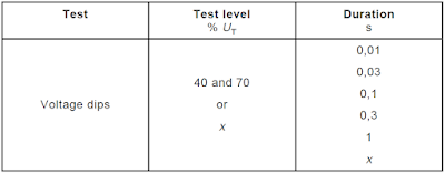
Code changes were implemented in the interruption tester for a closer approximation of EN 61000-4-29 and to improve the code portability between Infineon (Cypress) processors. In the EN 61000-4-29 standard, five tests are listed for DC voltage dips with fixed times of 10 ms to 1 s. An extract from the standard is shown below.

DC Voltage Dip Table from EN 61000-4-29

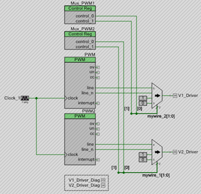
The PWM functionality in the Infineon microcontrollers, configured through the PWM component, was disabled.

Interrupt Tester Project Disabled PWM Logic

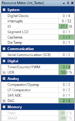
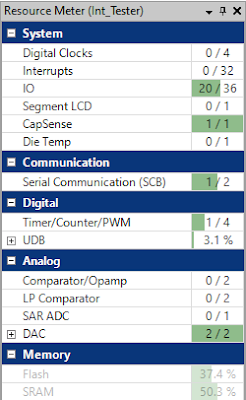
For the reduction in resources controlling the output pins between Cypress PWM and software output control, the Universal Digital Blocks (UDBs) dropped by almost 50 %.

Previous Project PSoC Resource Usage

Updated Project PSoC Resource Usage

The system timer was used as the replacement for the PWM component. Output pins that were PWM controlled are controlled directly in code. To improve the output waveform timing accuracy, the system timer was reconfigured from 10 ms to 1 ms.

Testing Code Changes
Timing control of the outputs controlling the load was performed in the corresponding function listed below.

/** *****************************************************************************
* Function Name: Output_Handler
*
* @brief Run interruption tests with timing below, 10 s separation between tests
*   Test 1 - 10 ms
*   Test 2 - 30 ms
*   Test 3 - 100 ms
*   Test 4 - 300 ms
*   Test 5 - 1000 ms
*
* @return none
****************************************************************************** */
void Output_Handler(uint8_t output_CurMenuItem, uint8_t out_statemachine)
{
    static uint8_t output_savedMenuItem;
    static uint8_t output_driver_state;
    
    if ((out_statemachine == OUTPUT_ON) && (output_CurMenuItem != 0))
    {       
        /* Handle PWM 1 Settings */
        if ((output_driver_state == OUT_OFF) || ((output_driver_state == OUT_LOW) && ( Pulse_Low_Ctr == 0)))
        {
            Pulse_High_Ctr = PWMValues[output_CurMenuItem].COMPARE1;
            Pulse_Low_Ctr = 0;
            output_driver_state = OUT_HIGH;
            V1_Driver_Write(true);
            V2_Driver_Write(true);
        }
        else if ((output_driver_state == OUT_HIGH) && ( Pulse_High_Ctr == 0))
        {
            Pulse_Low_Ctr = PWMValues[output_CurMenuItem].PERIOD1;
            output_driver_state = OUT_LOW;
            V1_Driver_Write(false);
        }
        output_savedMenuItem = output_CurMenuItem;
    }
    else if (out_statemachine != OUTPUT_ON)
    {
        V1_Driver_Write(false);
        V2_Driver_Write(false);
        output_driver_state = OUT_OFF;
    }
}


The standard EN 61000-4-29 standard states requirements for the rise and fall times when the tester is driving a 100 R load (
1 us to 50 us).

Test Generator Requirements from EN 61000-4-29

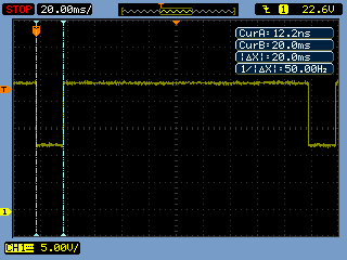
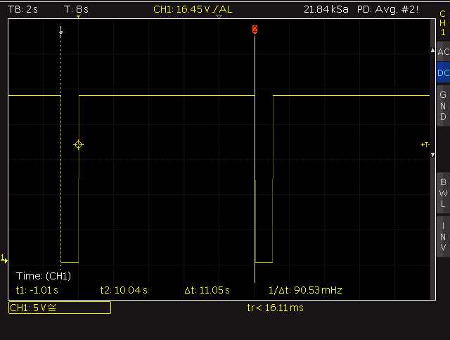
The pulse duration and time between tests were validated with the load.

10 ms Interruption Tester Output
 
100 ms Interruption Tester Output

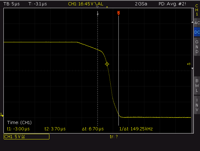
Testing showed that measured rise times were less than 18 us and the fall time less than 7 us.

Rise Time 10-90 % with 100 R Load

Fall Time 10-90 % with 100 R Load

Future Changes
To facilitate other microcontrollers, another revision of the display circuit board without capacitive sensing, a flat flex inter-board connection, watchdog and adding a third channel to the power board will be investigated.

Downloads
Listed below is the PSoC Creator project.

Interruption Tester 0.1c PSoC Project


Friday, 15 July 2022

Voltage Interruption Tester for IEC 61496-1 Part 5

Introduction
This blog continues from part 4 and finalised the supply voltage interruption tester (unit) post. 

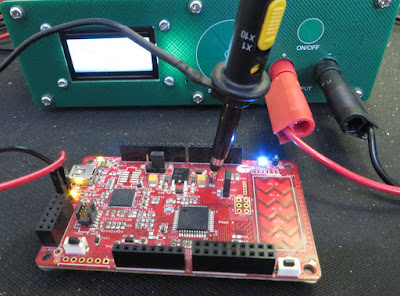
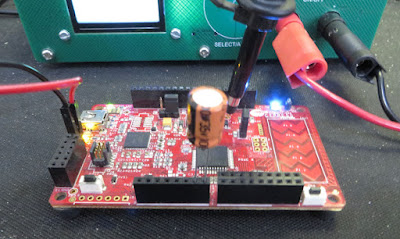
Covered in this blog is an interruption test applied to a PSoC development board. The test setup consisted of a Rigol DP832, the Interruption tester prototype and the PSoC development board part CY8CKIT-042.

Interruption Test Setup Using PSoC Development Board

This post also provides the source and Gerber files for the interruption tester project.

Practical Interruption Test

Disclaimer - The interruption test performed on the Cypress PSoC development board was performed for the sole purpose of measurement and testing only. The PSoC development board does not claim conformance with the test conducted.

Only interruption test 1 was performed because the operating voltage of the development board was stated as DC 5 – 12 V and the minimum operating voltage for the interruption tester output drivers is DC 8 V. Test 2 and 3 require half the supply voltage which was not practical.
For the program operating on the PSoC board, two outputs of a PWM block were used to separately toggle the onboard bi-colour LED.

When interruption test 1 was enabled, the 3.3 V supply was interrupted which resulted in the processor resetting. This is evident by the irregular operation of the bi-colour LED.


To resolve the issue caused by the dips in the supply rail, a 100 uF electrolytic capacitor was connected across the development board supply.


The two images below show a capture of the 3.3 V supply before and after the 100 uF capacitor was added to the development board.

Capture of Supply Rail During Interruption Test

Capture of Supply Rail During Interruption Test with Additional Capacitor

Shown in the image below is the location where the additional 100 uF capacitor was added to the development board.

Interruption Test Setup PSoC Development Board with Capacitor

While this test is straightforward on simple hardware, it shows the basic process behind interruption testing.

Final Comments
This series of blog posts focused on an overall view of the hardware design for the power supply interruption tester. While not every aspect of the design process was covered in detail, design files have been provided in the Downloads section to assist those interested in producing a similar project.

Downloads
Listed below are the PSoC Creator project, Gerber and BOM files for the Interruption Tester project. This project is supplied as shown in this blog (Posts 1 to 5).

Display Schematic and BOM

Display Gerber and NC Drill

Driver Schematic and BOM

Driver Gerber and NC Drill

Rear Panel Gerber and NC Drill

PSoC Creator Project (Complete Archived)


Sunday, 12 June 2022

Voltage Interruption Tester for IEC 61496-1 Part 4

Summary
This blog continues from part 3 of the supply voltage interruption tester (unit) post.

Covered in this blog are aspects of the Printed Circuit Board (PCB) implementation for the Infineon (Cypress) CapSense and output driver temperature measurements.
 
CapSense

CapSense has been available for over a decade however, I had not had a practical use for this technology on either a hobby or professional level until the interruption tester design. 

For the interruption tester, CapSense buttons were chosen instead of standard mechanical push buttons. During testing of the prototype interruption tester, daily variations in Capsense measurements were noted. While the variation resulted in sensitivity changes, tuning the CapSense component addressed most issues.

For the PCB layout, loosely following the CapSense PCB guidelines (Section 6.4) on a two-layer PCB resulted in poor performance. Tuning out interference or crosstalk was not achievable. This was likely due to the trace-to-trace spacing although the root cause was not investigated.

CapSense Trace-to-Trace Spacing - Courtesy Infineon

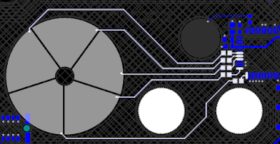
The design used in this blog uses a four-layer PCB with increased spacing between CapSense traces. For the 0.2 mm CapSense traces on the bottom layer, a 1.2 mm trace separation was used where practicable. Cross-channel triggering on CapSense lines no longer occured.

Interruption Tester - Radial Slider Trace-to-Trace Distance

Highlighted in the image below are the Capsense traces leading to the microcontroller for the radial slider.

Interruption Tester - Trace-to-Trace Spacing for Radial Slider

Output Driver Temperature Testing
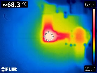
For tests 1 to 3, the high-side drivers (IPS160H) were driven into a resistive load to create a load of approximately 2.4 A. Temperature measurements were taken of the high-side driver(s) active for that test.

The test conditions for the various test are shown below.

Setup for Tests 1 to 3
Supply 1:
DC 24 V
Supply 2:
DC 12 V
Load: 10 R (resistive)
Test duration: 30 min
Ambient Temperature: Between 18
°C to 20 °C

Test 1 Results
Channel 1 IPS driver: 48
°C
Channel 1 Diode: 70
°C

Test 2 Results
Channel 1 IPS driver: 49
°C
Channel 1 Diode: 72
°C
Channel 2 IPS driver: 35
°C

Channel 2 Diode: 35
°C

Test 3 Results
Channel 1 IPS driver: 50
°C
Channel 1 Diode: 72
°C
Channel 2 IPS driver: 34 °C
Channel 2 Diode: 34
°C

Driver Temperatures

Test 1 - IPS Driver Temperature

 
Test 1 - Diode Temperature

The captures for the tests 2 to 3 were similar to those shown above for test 1. For heat dissipation the output drivers were mounted on the bottom of the PCB. Thermally conductive silicone pads can be used to move heat into the aluminum case of the Interruption Tester.

Setup for Test 5
Supply 1:
DC 12 V
Supply 2:
DC 60 V
Load: Transorb
Test duration: 1 min
Ambient Temperature:
20 °C

For test 5, a surface mount Transorb of unknown voltage was tested by attaching by short wires to the Interruption Tester.

Test 5 - Temperature of Transorb Under Test

While the output drivers showed little signs of heating, the Transorb heating was excessive.

Test 5 - Waveform Measurement across Transorb

The existing test duration of 100 Hz was changed as a result of this test.

More in post five

Saturday, 7 May 2022

Voltage Interruption Tester for IEC 61496-1 Part 3

Summary
This blog continues from part 2 of the supply voltage interruption tester (unit) post.

Covered in this blog is an overview of the unit assembly and code functionality.

Unit Assembly
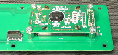
The display printed circuit board (PCB) contains a display (LCD) that requires mounting. The associated LCD hardware consists of M2.5 bolts, washers and spacers.

Interruption Tester Mounted LCD

For the connection between the display and power PCBs, surface mount connectors were used. Due to global supply constraints, this connector pair will be changed on a future PCB revision.

For the complete unit assembly, an anodised metal enclosure (Multicomp Pro MC002177) was utilised. The front and power PCB are fitted via the surface mount connectors and then slid into the enclosure. PCB slots are provided at various heights on the inside walls of the enclosure. To mount the front panel PCB, six bolts are required.

Interruption Tester Front Panel

The rear panel is placed over the banana connectors and held in place with a further six bolts.

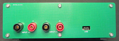
Interruption Tester Rear Panel

Rubber feet were fitted to complete the assembly.

Code Summary
The Infineon (Cypress) PSoC project is a standalone application targeted at the device CY8C4245AXI-483. The roadmap for the Interruption Tester project contains a firmware change to use the PSoC bootloader to suit field upgrades.

The project code is broken into three sections which relate to the user interface buttons, LCD and output drivers. These handlers interface with PSoC digital blocks by way of a system timer, Capsense, LCD, PWM and other interfaces.

PSoC Capsense Component
 

For the Capsense button handler, the 5-element radial Capsense (slider) value is processed which allows the selection of the LCD menu item.
The On/Off (Output) button is processed through a state machine that performs a latching/unlatching action on the button press. 
 

Capsense Scan Configuration

When the output is Off, the LCD presents a test number, that relates to the pre-programmed tests detailed in the following section. 

While the output is activated (On), the selection of other tests is not possible. The PWM blocks are programmed for continuous operations.

The display handler uses details from the button handler for the management of display strings.

PSoC LCD Component
PSoC LCD Component

The LCD has other tasks such as throwing up the boot screen or error states when applicable.

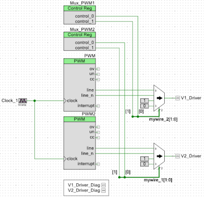
The output handler uses details from the button handler to configure PWM, configure the multiplexers and activate the high-side drivers. The two high-side drivers individually switch two input voltages, Voltage 1 (V1) and Voltage 2 (V2).

PSoC PWM and Multiplexer Components for Output Stage

Summary of Programmed Tests
Five tests are programmed with each test summarised below.

The term dipping, as described in the IEC standard, refers to the power supply changing voltage compared to interrupting which refers to the power supply switching OFF.

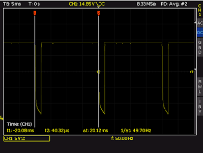
Test 1 - 10 ms pulse width interrupting Voltage 1 (V1) at a frequency of 10 Hz.  Voltage 1 is switched OFF.

Interruption Tester - Test 1 Output No Load

Test 2 - 20 ms pulse width dipping Voltage 1 (V1) at a frequency of 5Hz.  Voltage 1 is switched OFF and Voltage 2 will be supplied during V1 off time.

Interruption Tester - Test 2 Output No Load

Test 3 - 500 ms pulse width dipping in Voltage 1 (V1) at a frequency of 0.2 Hz.  Voltage 1 is switched OFF and Voltage 2 will be supplied during V1 off time.

Interruption Tester - Test 3 Output No Load

Test 4 – 1.8 ms pulse width dips in Voltage 1 (V1) at a frequency of 50 Hz. Voltage 1 is switched OFF.

Interruption Tester - Test 4 Output No Load

Test 5 – Approximately 280 us pulse width (spikes) at a frequency of 100 Hz. Voltage 1 remains ON and Voltage 2 will be switched ON to generate the spike.

Interruption Tester - Test 5 Output No Load

The IEC standard states that the equipment under test (EUT) should be subject to ten dips. Updates to the code could allow for the dips to be limited to ten. The tests currently continue to run.

Tests 1 through 3 allow for basic testing to the IEC standard.

Test 4 was created for verifying filters targeting 50 Hz.

Test 5 can be used with an oscilloscope to check the performance of devices and designs using protection diodes. These diodes may include steering or Transient (Tranzorbs) diodes. A narrow pulse (spike) is applied for a short time at a frequency of 100 Hz. The frequency may need to be adjusted for applications where the protection diodes are low power.

Tests 1 and 2 are classified as B tests meaning that the operation of the EUT should not be changed as a result of the test. Test 3 is classified as a C-test which means that the EUT can fail in a known condition.

More in post four

Saturday, 23 April 2022

Voltage Interruption Tester for IEC 61496-1 Part 2

Summary
This blog follows a previous post where the concept for a supply voltage interruption tester (unit) was validated.

In this blog, the design was formalised by implementing the design on circuit boards using available electronic components. The alternate design supports operating voltages from DC 8 V to 60 V at 2.5 A.

Voltage Interruption Tester Prototype

The design goal was to create a cost-effective unit that would provide indicative testing for Section 4.3.2.2 Supply Voltage Interruptions of the standard IEC 61496-1. The testing is indicative because this units is not an IEC qualified unit.

Two external power supplies supply the voltages that are switched by the unit to generate the required output waveforms.

In addition to the standard IEC tests, two additional tests were added; one for generating repetitive mains frequency noise (50 Hz) and the second for testing diodes such as Transient (TVS).

Example Output Waveform from Voltage Interruption Tester

Editing the project source could yield additional or completely new tests.

Hardware Overview
Three circuit boards (PCB) were created. These consisted of a front, rear and internal PCB. For ease of use on the bench, the design was made to suit a small aluminium enclosure. The two boards containing electronic devices detailed below.

Power PCB Prototype
Power PCB Prototype (Top Side)

The first board, labelled the power board, contained a DC 3.3V regulator with an operating range of DC 4 to 60 V, high side drivers, pluggable power banana connectors and an optional USB interface. The high side driver operating voltage is DC 8 to 60V.

Power PCB Prototype
Power PCB Prototype (Bottom Side)

The front PCB was also purposed as the unit's panel. This board contained a Cypress microcontroller and a two-line LCD.

Display PCB Prototype
Display PCB Prototype (Bottom Side)

Buttons were implemented on the PCB using the Cypress Capsense interface.

Display PCB Prototype
Display PCB Prototype (Top Side)


Power PCB
The power PCB was created as a double-sided board so that the two high side switches (IPS160H) could take advantage of heat dissipation to the aluminium case if needed. Signals from the high-side switches were provided to the microcontroller although monitoring was not implemented at this time.

PCB mount banana plugs provided the connections for the dual supply inputs and voltage interruption tester output.

Powering of the microcontroller and LCD on the display PCB was realised using a DC 3.3 V wide operating range DC-DC switchmode (LMR16006XD). The switchmode will begin operating with an input voltage of 3.6 V which may be useful for high side switches with a lower operating voltage.

Debug and diagnostic feedback were provided through an optional USB interface.

A resistor population option allows for the selection of the switchmode supply source. This could either be input voltage 1, 2 or the optional USB.

Display PCB
Contained on the display PCB were the microcontroller and two-line LCD.

Prototype Supply Interruption Tester LCD

An interface for the operator was achieved using PSoC Capsense buttons. Capsense signals were interfaced to the Cypress microcontroller providing a five-element radial slider and an On/Off button. The cross-hatching pattern seen on the PCB significantly helps with the Capsense operation.

Rear PCB
There were no components mounted on the rear PCB however the front and rear PCBs used the silkscreen to provide the relevant operational information.
 
Rear PCB Prototype
Rear PCB Prototype
 
 
Continued in Part 3

Thursday, 29 April 2021

Novel Voltage Interruption Tester for IEC 61496-1

Summary
This blog provides details of a novel voltage interruption tester that demonstrates the requirements listed in the IEC 61496-1 standard, section 4.3.2.2. 

The tester was needed because certain types of electronic hardware must be tested to the IEC 61496-1 standard and dedicated testing facilities have had reduced access during the pandemic. The purpose of the tester in this blog is preliminary testing which would not replace an authorised testing facility.

Description
The interruption test hardware described in this blog was designed for DC systems to 48 V and currents to 3 A. For design constraints, interruption timing was considered important, followed by access to available hardware then output voltage regulation.

The capture below displays section 4.3.2.2 of the IEC standard which shows the timing of the three interruption tests.

Supply Voltage Interruptions

Hardware Solutions
Off the shelf power supply evaluation boards such as the Vishay SiC461 were tested initially. To control the output voltage, a programmable resistor replaced one of the feedback elements. By using a programmable resistor, a 10 ms pulse width was achievable. However, the output voltage rise and fall times were asymmetrical and several milliseconds in duration.

Alternative solutions utilising linear regulators such as the LM317T were analysed. The linear regulator produced very sharp output voltage rise and fall times. The limitation of the linear regulator was the LM317 voltage regulation and accompanying device heat dissipation.

By utilising existing resources, such as individual benchtop supplies, a simpler solution was identified. It was likely that workspaces would have access to one dual output or two single regulated adjustable power supplies. These supplies could be used together for the switching tests.

The hardware in the system consisted of a microcontroller (PSoC) that interfaced to a pair of optocouplers (4N28) in turn driving two high-side switches (BTS50085). The output of each high-side switch was tied together with series diodes (1N5404) to produce the output.

One design weakness using this solution was the supply to output voltage drop. As the cumulative voltage drop of the high-side switch and diode changed with load current, the power supplies required adjustment to achieve the correct test voltages.

Hardware Concept
Shown below was the original concept proof of the hardware. The high-side switch datasheet lists an operating voltage to some 58 V and a current of 11 A.

Interruption Tester Concept Hardware


Circuit Overview
Control signals generation was performed by a microcontroller; any type could perform the task as the signals are slow-moving. Two control signals from the microcontroller drive a set of optocouplers. For this design, an ancient pair of 4N28’s were fitted. 

The transistor output of the optocouplers switched the high-side driver inputs to 0 V. This was required as the inputs of the high-side drivers BTS50085 must be switched to 0 V to activate their outputs.

Microcontroller
An off the shelf CY8CKIT-059 Cypress development board implemented a PWM to drive two outputs for the optocouplers. 

The onboard switch and LED acted as the user interface. 

Repetitive switch presses selected a subsequent test. Flashes from the onboard blue LED indicated the test number. No flash for off, one flash for test one up to three flashes for test three.

For the top design in PSoC Creator, the first PWM output provided the timing for the voltage dip. The second PWM output configuration and some flip flops ensured that the half voltage was active before and after the first PWM changed state. Understandably there are other ways to use the PWM component, again this was a concept proof.

PSoC Creator PWM Test Setup

The PWM was configured as illustrated below. Settings were controlled from within the code.

PWM Component Setup
PWM Component Setup


The rise and fall times (10%, 90%) were 20 us and 90 us respectively
with the output driving a resistive load.

Rise Time for Resistive Load

Fall Time for Resistive Load

Output Waveforms
The following captures were taken when driving a resistive load.
 

Interruption Test 1 with Resistive Load
 

Interruption Test 2 with Resistive Load


Interruption Test 3 with Resistive Load

The next captures were taken when driving a DC 12 V fan.

Interruption Test 1 with DC Fan

Interruption Test 2 with DC Fan

Interruption Test 3 with DC Fan

Output Voltages
For the three interruption tests, various loads were tested and peak voltages measured.
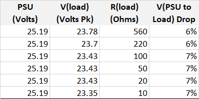
Interruption Test 1 with Various Resistive Loads

Interruption Test 2 with Various Resistive Loads

Interruption Test 3 with Various Resistive Loads
 

The above test results show that adjustment to the power supply voltages was required to accommodate for the system voltage drop.

PSoC Code
Listed below is the test code for the PSoC controller.


/**
* @file main.c
* @brief Basic example of IEC61496-1 tests
* @version 0
*
* History
* Version       Change Notes
* 0.0           Test code
*/

#include <project.h>
#include <stdbool.h>

/* Prototypes */
void led_flash_state(uint8 state_num);


/**
* @brief Flash LED
* @param state
*/
void led_flash_state(uint8 state_num)
{   
    while (state_num != 0)
    {
        LED_Write(true);
        CyDelay(250);
        LED_Write(false);
        CyDelay(250);
        state_num--;
    }
}

/**
* Main
*/
int main()
{                       CyGlobalIntEnable;

    
uint8 state = 0;
    uint8 state_update = false;
    
    for(;;)
    
{
    if (SW1_Read()== false)
    {
        CyDelay(200);         /* Some debounce */
        
state++;
        state_update = false;
        if (state == 4)      /* Toggle states */
        {
            state = 0;
        }
    }

    if ((state == 0) && (state_update == false))
    {
        PWM_Stop();
        state_update = true;          /* No PWM in first state */
    }
    
    if ((state == 1) && (state_update == false))
    {
        PWM_Stop();                     /* Test 1 - 10 ms 100% dip */
        PWM_WritePeriod(999u);
        PWM_WriteCompare1(110u);        /* Control PWM output 1 */  
    
    PWM_WriteCompare2(0u);
        PWM_WriteControlRegister(PWM_CTRL_ENABLE);
        PWM_Start();
        led_flash_state(state);
        state_update = true;
    }

    if ((state == 2) && (state_update == false))
    {
        PWM_Stop();                      /* Test 2 - 20 ms 50% dip */
        PWM_WritePeriod(1999u);
        PWM_WriteCompare1(200u);
        PWM_WriteCompare2(210u);         /* Control PWM output 2 for lower voltage */         PWM_Start();
        led_flash_state(state);
        state_update = true;
    }

    
if ((state == 3) && (state_update == false))
    {
        PWM_Stop();                      /* Test 3 - 500 ms 50% dip */
        PWM_WritePeriod(49999u);
        PWM_WriteCompare1(5000u);
        PWM_WriteCompare2(5010u);        /* Control PWM output 2 for lower voltage */         led_flash_state(state);
        state_update = true;
    }
  }
}

/* End */


Summary
For concept proof, the tests using high-side switches controlled by a microcontroller verified specific requirements detailed in the IEC 61496-1 standard. During tests, the input to output voltage drop was less than 10 %. Compensation for voltage drop was achieved by adjusting power supply voltages.

Depending on design requirements, a different microcontroller, high-side switches with a lower operating voltage, or alternative components could be selected. If isolation from the switched output voltage was not a consideration, the optocouplers could be omitted.

With access to testing facilities being limited, having the hardware to provide preliminary on bench verification can be a consolation.

Downloads
The PSoC Creator 4.4 project and schematic from the Top Design are available for download.

PSoC Creator Top Design Schematic

PSoC Creator 4.4 Project