Showing posts with label silicon. Show all posts

Wednesday, 13 July 2022

PSoC Silicon ID Header File Creation

Summary
This blog offers a solution to generate PSoC header files from Cypress DAT files using PowerShell scripts. Available Cypress DAT files are merged and then converted into a single header file.

There is a thread similar to this post on the Infineon website called ‘JTAG/Silicon ID reference file’.

History
Fluctuations in global chip levels have resulted in a wider range of microcontrollers seen by companies responsible for programming and testing electronic hardware. 

To accommodate changes in microcontrollers using a more automated process for creating software header files, the scripts mentioned in this blog were designed. These scripts are fully functional, however, not without limitations as this is an initial foray into splitting scripts with this type of file content manipulation. 

The scripts were written in two parts because one script was made to run in the Program Files directory that contains the relevant DAT files. The second script was made to run with the merged DAT file.

Installation Requirement
To access the DAT files, the Cypress (Infineon) PSoC Programmer should be installed. The DAT files are located at the following location - C:\Program Files (x86)\Cypress\Programmer\Devices
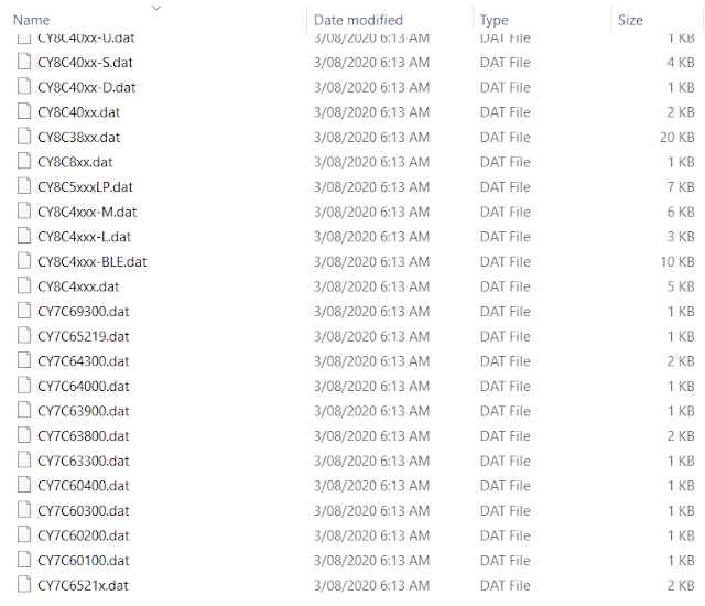
Example of Cypress .DAT File Listing

The DAT files contain various items of PSoC information. Of this, the device name and ID range are of primary interest. 

As an example for PSoC device CY8C4125AZI-473, the entry from file CY8C4xxx.dat is displayed below.

2,CY8C4125AZI-473, CY8C4125AZI-473, 48, 32768, 3, 04_2B_11_93, 04_2B_12_93, v33


Whether the PSoC ID is utilised to program PSoC devices or other information such as the size of the flash is needed for programming file verification, the PowerShell script could easily be adapted to suit these purposes.

Implementation
The first script called 'dat_merger.ps1' combines multiple DAT files using the PowerShell add-content command. The script was designed to handle all DAT files in the Cypress Programmer Devices directory however the script will also work on a single DAT file. 

Additionally, the first row in each DAT file is removed since this is redundant. To process the file in the next script, the merged file is saved in CSV format.

$dir = Get-Location
Write-Host "Merging Files"

$source ="$dir\*.dat"
$destination = "$dir\merge.csv"

# Remove first row and merge all files in directory
Get-ChildItem -Filter '*.dat' | ForEach-Object {
Get-Content $_ | Select -Skip 1 | Add-Content $destination
}


The second script dat_parser.ps1 removes any unwanted columns, selects only the first column of PSoC IDs, adds the text ‘#define’, formats the ID into a preferred value by stripping the formatting and then saves the result as a jtag.h file.

$dir = Get-Location
Write-Host "Parsing files in $dir"
# Grab merged csv files
$source = "$dir\merge.csv"
$destination ="$dir\jtag.h"

# Strip columns, add hash define and number format for each line, strip CSV then save as header file
Import-CSV-Delim ','$source -Header a,b, c, d, e, f, g |
Select "b","g" | ForEach-Object {$_."b" = "#define $($_."b")";$_} |
ForEach-Object {$_."g" = "0x$($_."g")";$_} |
ConvertTo-Csv -NoTypeInformation |
Select-Object -Skip 1 |
# Option for tab instead of spaces
#% { $_ -replace ‘_‘, “” -replace (‘,‘, "`t")  -replace ('"', '')} |
% { $_ -replace _‘, “” -replace (‘,‘, ''.padleft(10, ' '))  -replace ('"','')} |
Out-File $destination -Encoding utf8


Output
The first script would merge DAT files. Two example files were chosen CY8C42xx-D.dat and CY8C44xx.dat.

Before Script 

1,CY8C42xx-D, CY8C42xx-D, 8, 5, 128
2,CY8C4245PVI-DS402, CY8C4245PVI-DS402, 28, 32768, 3, 17_03_11_A7, v17
2,CY8C4245FNI-DS402, CY8C4245FNI-DS402, 25, 32768, 3, 17_02_11_A7, v17
2,CY8C4246PVI-DS402, CY8C4246PVI-DS402, 28, 65536, 3, 17_01_11_A7, v17
2,CY8C4246FNI-DS402, CY8C4246FNI-DS402, 25, 65536, 3, 17_00_11_A7, v17

1,CY8C44xx, CY8C44xx, 8, 5, 128
2,CY8C4A45PVI-481, CY8C4A45PVI-481, 28, 32768, 3, 1C_02_11_AC, v17
2,CY8C4A45FNI-483, CY8C4A45FNI-483, 45, 32768, 3, 1C_03_11_AC, v17
2,CY8C4A45LQI-483, CY8C4A45LQI-483, 48, 32768, 3, 1C_00_11_AC, v17
2,CY8C4A45AZI-483, CY8C4A45AZI-483, 48, 32768, 3, 1C_01_11_AC, v17
2,CY8C4A45FNQ-483, CY8C4A45FNQ-483, 45, 32768, 3, 1C_41_11_AC, v17
2,CY8C4A45LQQ-483, CY8C4A45LQQ-483, 48, 32768, 3, 1C_40_11_AC, v17

After Script 
2,CY8C4245PVI-DS402, CY8C4245PVI-DS402, 28, 32768, 3, 17_03_11_A7, v17
2,CY8C4245FNI-DS402, CY8C4245FNI-DS402, 25, 32768, 3, 17_02_11_A7, v17
2,CY8C4246PVI-DS402, CY8C4246PVI-DS402, 28, 65536, 3, 17_01_11_A7, v17
2,CY8C4246FNI-DS402, CY8C4246FNI-DS402, 25, 65536, 3, 17_00_11_A7, v17
2,CY8C4A45PVI-481, CY8C4A45PVI-481, 28, 32768, 3, 1C_02_11_AC, v17
2,CY8C4A45FNI-483, CY8C4A45FNI-483, 45, 32768, 3, 1C_03_11_AC, v17
2,CY8C4A45LQI-483, CY8C4A45LQI-483, 48, 32768, 3, 1C_00_11_AC, v17
2,CY8C4A45AZI-483, CY8C4A45AZI-483, 48, 32768, 3, 1C_01_11_AC, v17
2,CY8C4A45FNQ-483, CY8C4A45FNQ-483, 45, 32768, 3, 1C_41_11_AC, v17
2,CY8C4A45LQQ-483, CY8C4A45LQQ-483, 48, 32768, 3, 1C_40_11_AC, v17


Running the second script on the merged file output from the first script results in a new file called jtag.h as shown below.

#define CY8C4245PVI-DS402         0x170311A7
#define CY8C4245FNI-DS402         0x170211A7
#define CY8C4246PVI-DS402         0x170111A7
#define CY8C4246FNI-DS402         0x170011A7
#define CY8C4A45PVI-481         0x1C0211AC
#define CY8C4A45FNI-483         0x1C0311AC
#define CY8C4A45LQI-483         0x1C0011AC
#define CY8C4A45AZI-483         0x1C0111AC
#define CY8C4A45FNQ-483         0x1C4111AC
#define CY8C4A45LQQ-483         0x1C4011AC

One of the limitations with the current implementation is the uneven padding between the PSoC device name and the ID. The parser code inserts ten white spaces which may not conform with all programming styles.

Final Thoughts
The PowerShell scripts (under GPL) have been tested on several DAT files however the outputs should be verified as part of standard practice. Improvements are welcomed!

Downloads
 

Cypress Dat Merger PowerShell Script
dat_merger.ps1

Cypress Dat Merger PowerShell Script
dat_parser.ps1

Cypress Dat Merger PowerShell Script
jtag.h
(Example of PSoC4, PSoC5)


Thursday, 16 August 2018

Silicon Labs SI8380S example design

Summary
This blog details the design and testing of a circuit board 'PCB' for the Silicon Labs SI8380S Digital Isolator PLC input device. The circuit board was designed to use the Arduino compatible pin layout with the code developed for the Cypress CY8CKIT-042 development board using PSoC Creator.

Silicon Labs Digital Isolator
In a previous blog, the approach of implementing PLC inputs using discrete components was reviewed for Single Board Computer such as the Raspberry Pi and Beagle. The use of the Silicon Labs eight input digital isolator could be considered a progression on the discrete solution. Some benefits in using the digital isolator pertain to component count reduction, localised solution, and the option of using a serial interface (SPI).

Schematic Design
Silicon Labs provide a basic application schematic in Application Note 970 which serves as a starting point for the design.


Silicon Labs Example Application Schematic
Silicon Labs Example Application Schematic
The Silicon Labs device datasheet and the aforementioned application note also detail resistor values for achieving the necessary IEC PLC Input Types from 1 to 3.


Silicon Labs Suggested Resistor Values
Even though there is little mention of input protection for the design, additional parts were included on the Arduino compatible board for the purposes of testing.


Silicon Labs Alternative PLC Input Section
The schematic displayed above was designed for testing five possible input circuit configurations. Some parts in the schematic are superfluous because of the technology used inside the Silicon Labs device. This is explained later in the blog.

1. Diodes - D1, D2, D3 not fitted. D2 replaced with a zero ohm link. This design is representative of the Silicon Labs design.

2. Diodes - D1, D3 not fitted. Using a single forward biased diode would commonly provide reverse polarity protection for a PLC input circuit. When a diode is used on the test PCB, the bipolar input behaves as a unipolar input in a sinking configuration. No overvoltage protection would be provided to the input of the Silicon Labs device.

3. Diode - D2 not fitted. Using the series Zener reduces the power dissipation in the resistors and provides overvoltage protection for the input of the Silicon Labs device. The inclusion of the series Zener also changes the turn ON and OFF characteristics of the circuit.

4. Diodes - D1, D2 not fitted. D2 replaced with a zero ohm link. The design provides overvoltage protection for the input of the Silicon Labs device and retains the turn ON and OFF characteristics of the circuit.

5. Diode - D1 not fitted. The design provides overvoltage with the Zener and would commonly provide reverse polarity protection. The series Schottky diode would only result in a slight deviation in turn ON and OFF characteristics of the circuit because the low forward drop of a Schottky.

Capacitor C3 was added for signal conditioning.


Arduino Pin Compatible Silicon Labs Adaptor Design
PCB Design
The board layout and connector placement was borrowed from an Arduino Uno board and verified against the Cypress CY8CKIT-042 development board.


Arduino Pin Compatible 8 Input Silicon Labs Prototype PCB
Some prior checking using a Cypress Creator project was required to ensure that the pins chosen for SPI communications would be compatible with the Cypress SPI component and the development board.

PCB Population
Only relevant components and a single input channel were populated for initial testing of the PLC prototype PCB. The image below shows the unpopulated prototype.


Prototype PCB for Silicon Labs SI8380S
Obligatory test points were soldered to the board to observe the data exchange on SPI with the Silicon Labs device. 

Cypress Development Board
A connection for a UART was added on the Cypress development board. A connection was made between the on-board PSoC4 and PSoC5 (Kitprog) devices to provide debug information during code development.

Arduino Pin Compatible 8 Input Silicon Labs Constructed Prototype
Silicon Labs Prototype Input Circuit 1
For the following tests conducted, a series of measurements were taken with tabulated data detailed after the last test.

Testing Input Circuit 1
As shown in the above capture only resistors R1 and R2 were fitted to the prototype, with input diode D2 replaced with a zero ohm link.

Turn on 7.7VDC and Turn off 7.1VDC

Testing Input Circuit 2
As shown in the capture below, diode D2 and resistors R1 and R2 were fitted to the prototype.

Turn on 7.9VDC and Turn off 7.3VDC


Silicon Labs Prototype Input Circuit
Silicon Labs Prototype Input Circuit 2
Testing Input Circuit 3
As shown in the next capture below, diodes D1, D2 and resistors R1, R2 were fitted to the prototype.

Turn on 12.8VDC and Turn off 12.2VDC


Silicon Labs Prototype Input Circuit
Silicon Labs Prototype Input Circuit 3
Testing Input Circuit 4
As shown in the next capture below, diode D3 and resistors R1, R2 were fitted to the prototype. Diodes D1 and D2 were not fitted and D2 was replaced with a zero ohm link.

Turn on 7.7VDC and Turn off 7.1VDC


Silicon Labs Prototype Input Circuit
Silicon Labs Prototype Input Circuit 4
Testing Input Circuit 5
As shown in the last capture below, diodes D2, D3 and resistors R1, R2 were fitted to the prototype. Diode D1 was not fitted.

Turn on 7.9VDC and Turn off 7.3VDC


Silicon Labs Prototype Input Circuit
Silicon Labs Prototype Input Circuit 5


Input Circuit Initial Measurement Data
As expected only input circuit 3, with the series Zener D1 on the input, was significantly different. One item to note is the reduction in total resistor power dissipation due to the addition of the Zener.

The diodes used for testing were manufactured by Diodes Incorporated. The Zener diodes being part BZT52C5V1 and the Schottky diode part SBR1A40S3. All resistors were from ROHM in a 1206 case, rated at 500mW.

Modified Input Circuit 3
The range of Silicon Labs PLC input devices are compliant to the IEC_61131-2:2003 standard. To modify the input circuit 3 with the Zener diode the turn On voltage was reduced. The IEC_61131-2 standard for a Type 3 input specifies 11V to 30V for a 'Signal 1' or logic high.


Silicon Labs Prototype Input Circuit
Silicon Labs Prototype Input Circuit 3 - Modified
Resistor R2 was reduced from 2k7 to 1k8 by placing a 5k62 resistor in parallel, as shown in the capture above. The same series of measurements were performed with the modified input circuit. Tabulated data with the modified input, 3 Mod, is shown below.


Input Circuit Measurement Data
Using the 1k8 resistor was not ideal because the measured voltage for Turn On is close to the 11V required by the IEC standard. Changing R1 and R2 may provide a better result with respect to the requirements of the IEC standard.

PSoC SPI 
A PSoC Creator project was used to read data from the SI8380S using either SCB or UDB components. The default project settings could possibly be modified for faster performance of the SPI. System clock for example could be increase from 24MHz to the maximum 48MHz. 

For an example, a signal generator set at 10 kHz with a DC offset was used to drive the SI8380S. The green trace in the capture below shows the output of the signal generator. The yellow trace is an output pin on the PSoC which is driven in response to the SI830S data.


Silicon Labs SI8380S PSoC Signals - Turn ON Delay

The listing below shows the code used for initial testing.


/*******************************************************************************
* File Name: main.c
*
* Version: 1.0
*
* Description:
* This example project demonstrates the use of the Silicon Labs SI8380S
* https://www.silabs.com/documents/public/data-sheets/Si838x-DataSheet.pdf
*
* Hardware Connections
* MOSI  P0.4
* MISO  P0.5
* SCK   P0.6
* SS    P0.7
*
*******************************************************************************/
#include <main.h>
#include <stdbool.h>

/* Defines for SI8380S registers */
#define SI8380_CHAN_STATUS      0x0             /* Status of the eight PLC inputs */          
#define SI8380_DBNC_MODE0       0x1             /* Mode control bits for the first four channel debounce filters */
#define SI8380_DBNC_MODE1       0x2             /* Mode control bits for the second four channel debounce filters */
#define SI8303_DBNC_DLY0        0x3             /* Delay control bits for the first four channel debounce filters */
#define SI8380_DBNC_DLY1        0x4             /* Delay control bits for the second four channel debounce filters */

/* Define bits used in control bytes */
#define DELAY_0MS               0x00
#define DELAY_10MS              0x01
#define DELAY_30MS              0x10
#define DELAY_100MS             0x11
#define DBNC_NO_FILTER          0x00
#define DBNC_LP_FILTER          0x01
#define DBNC_LEADEDGE_FILTER    0x10
#define SI8380S_BRCT            0x80            /* Broadcast = 1, Address a device = 0 */
#define SI8380S_RW              0x40            /* Read = 1, Write = 0 */

/* Define UDB or SCB */
#define SCB_BLOCK_USED                        /* 0.24 Mbps with x 10 sampling */
//#define UDB_SPI_BLOCK                           /* 6 Mbps max */
#define debug                                 /* Transmit only to terminal at 115200, 8, N, 1 */

/* SPI registers */
uint8 SI8380S_Control;
uint8 SI8380S_Address;
uint8 SI8380S_R_Data;
uint8 SI8380S_W_Data;


/* Function prototypes */
uint8 SI8380S_Read(uint8 spi_r_control, uint8 spi_r_address);
void SI8380S_Write(uint8 spi_w_control, uint8 spi_w_address, uint8 spi_w_data);


/*******************************************************************************
* Function Name: SI8380S_Read
*******************************************************************************/
uint8 SI8380S_Read(uint8 spi_r_control, uint8 spi_r_address)
{
    uint8 data_temp_buf;

    #ifdef SCB_BLOCK_USED
        SPIM_SpiUartWriteTxData(spi_r_control);
        SPIM_SpiUartWriteTxData(spi_r_address);
        SPIM_SpiUartWriteTxData(0x00);   
        // init task timeout
        while (SPIM_SpiUartGetRxBufferSize() == 0);                 /* Has any data been received */
        // reset task timeout
        data_temp_buf = SPIM_SpiUartReadRxData();
    #endif

    #ifdef UDB_SPI_BLOCK
        SPIM_WriteTxData(spi_r_control);
        // init task timeout
        while (!(SPIM_ReadTxStatus() & SPIM_STS_BYTE_COMPLETE));    /* Wait until byte complete to reassert Slave Select */
        // reset task timeout
        // init task timeout
        SPIM_WriteTxData(spi_r_address);
        while (!(SPIM_ReadTxStatus() & SPIM_STS_BYTE_COMPLETE));    /* Only continuous mode for a UDB component  */
        // reset task timeout
        // init task timeout
        SPIM_WriteTxData(0x00);
        while (!(SPIM_ReadTxStatus() & SPIM_STS_BYTE_COMPLETE));    /* SCB component may be more suitable */       
        // reset task timeout
        // init task timeout
        while (SPIM_GetRxBufferSize() == 0);                        /* Has any data been received */
        // reset task timeout
        data_temp_buf = SPIM_ReadRxData();   
    #endif

    return data_temp_buf;
}

/*******************************************************************************
* Function Name: SI8380S_Write
*******************************************************************************/
void SI8380S_Write(uint8 spi_w_control, uint8 spi_w_address, uint8 spi_w_data)
{
    #ifdef SCB_BLOCK_USED
        SPIM_SpiUartWriteTxData(spi_w_control);
        SPIM_SpiUartWriteTxData(spi_w_address);
        SPIM_SpiUartWriteTxData(spi_w_data);
        // init task timeout
        while (SPIM_SpiUartGetRxBufferSize() == 0);                 /* Has any data been received */
        // reset task timeout
    #endif

    #ifdef UDB_SPI_BLOCK
        // init task timeout
        SPIM_WriteTxData(spi_w_control);
        while (!(SPIM_ReadTxStatus() & SPIM_STS_BYTE_COMPLETE));
        // reset task timeout
        // init task timeout
        SPIM_WriteTxData(spi_w_address);
        while (!(SPIM_ReadTxStatus() & SPIM_STS_BYTE_COMPLETE));
        // reset task timeout
        // init task timeout
        SPIM_WriteTxData(spi_w_data);
        while (!(SPIM_ReadTxStatus() & SPIM_STS_BYTE_COMPLETE));
        // reset task timeout
    #endif
}

/*******************************************************************************
* Function Name: main
*******************************************************************************/
int main()
{
    /* Start components */
    spim_sck_Write(false);
    CyDelay(1);
    Spim_sck_Write(true);                                              /* Resync the SI8380 state machine */
    SPIM_Start();
    UART_Start();
    CyGlobalIntEnable;
    UART_PutString("Start\r\n");
    uint8 channel_data, channel_data_old = 0;
    for(;;)
    {
        channel_data = SI8380S_Read(SI8380S_RW, SI8380_CHAN_STATUS);    /* Update data */
        #ifdef debug
         if (channel_data != channel_data_old)
         {
            UART_PutChar(channel_data);      /* Read data continuously */
            CyDelay(250);
            channel_data = channel_data_old;
         }
        #endif
    }
}
/* [] END OF FILE */


Completed PCB 
The PCB was loaded with a single Schottky diode and the two resistors associated with the divider for each input.


Silicon Labs Prototype - Completed
Testing was conducted with RealTerm acting as the terminal monitor.


Silicon Labs Prototype - Serial Monitor Output
Each input was turned ON in sequence to prove operation.

Excessive Input Voltages
As a final destructive test the input voltage to the board was increased from 24V DC in 2V steps until system failure. All PLC inputs were configured as type 2, series diode and resistor divider only.

A Rigol DP832 was used to increase the voltage with voltage measurements performed at the PLC input connector of the prototype board. Results for the measurements are shown below.


Prototype PLC: Input Voltage vs SI8380S AHx Voltage
Graphed results for the above measurements.


Prototype PLC: Graphed Input Voltage vs SI8380S AHx Voltage Results
At some voltage above 62V DC the SI8380S ceased SPI communications with the Cypress controller. When the cause of failure could not be determined the SI8380S was replaced and operation was confirmed again at 24V DC. The second device was not provided with more than 60V DC consequently the SI8380S may operate with higher input voltages.

Summary
For a minimal external support component count, the range of Silicon Labs isolated PLC input isolators is an obvious rival to similar devices available in the market.

The limited testing in this blog showed more than acceptable performance with a single Silicon Labs SI8380S over a range of input voltages from 24V to 60V DC with the SPI interface. 

Isolation voltages were not tested or verified in this blog.

Downloads
PLC Input Schematic
PLC Input Schematic
PLC Input Gerbers
PLC Input Gerbers

PSoC Creator 4.2 Silicon Labs Project