Introduction
This blog discusses a few options that new circuit board designers may use for return path vias as a result of signal traces changing circuit board layers through using vias.
Further Literature
It is highly recommended that existing content from industry figures such as Eric Bogatin or Rick Hartley are reviewed. Related circuit board information is available from YouTuber channels such as Robert Feranec or Phils Lab to mention a few.
PCB Routing Example
For circuit board designs that feature microcontrollers, microprocessors, FPGA or similar devices with high pin count or spacing density the existing connections to power rails through vias can serve as return paths. In the image below, taken from the Altium Mini-PC board, the green highlighted vias indicate the several 0V (GND) power connections that may function as return paths for the DDR memory address, data, clock and control signals.
 |
| Altium Mini-PC Board Highlighted GND (0V) Vias (Courtesy Altium) |
Reducing Return Path Distance
The capture below is a further extract from the Mini-PC demonstration board showing a distance measurement between a return via and a differential DDR clock pair.
A Texas Instruments Application Note, High-Speed Interface Layout Guidelines, 2023 states that the signal to return via distance should be a maximum distance of 5 mm (200 mil) although that value could be considered design dependent. For the Mini-PC demonstration board, the distance between the return via and differential pair is small, some 2.1 mm.
 |
| Altium Mini-PC Board Differential Via Pair (Courtesy Altium) |
Consider a situation where the return path distances needed to be reduced. On the Mini-PC board, a smaller distance could be achieved following a circuit board review. Traces on the layers could be moved to make room for a via closer to the differential via pair. The capture below shows one possible change with a reduction to 1.4 mm.
 | |
|
Board Space Limitations
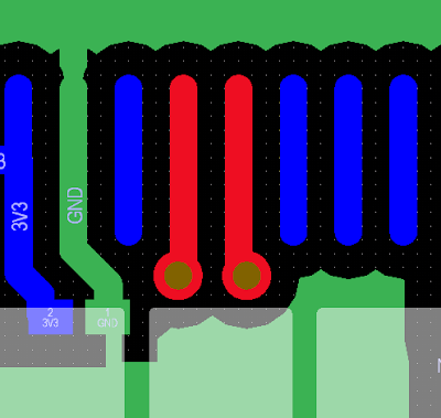
A more common limitation when adding or altering return path vias could be related to circuit board space. In the example below, the traces in the red colour identify a differential pair. There is no return path via in close proximity. The while highlighted rectangles represent pads on the other side of the circuit board.
 |
| Differential Pair with No Return Path Via on a Double Sided Circuit Board |
The reason for no return path via in the area is two-fold. On the opposite side of the circuit board is a surface mount component with large pads making return via placement difficult. The second limitation is due to the PCB rules. The smallest via hole size is configured for 0.3 mm.
The limitation created by the component on the opposite side can be overcome using a number of solutions. Using the existing circuit board via the size of 0.3/0.5 mm (via hole size/via diameter) three vias could be placed onto the circuit board as shown below. This solution yields a differential pair to return path via distance of 2.3 mm.
 |
| Differential Pair with Three Return Path Vias on a Double Sided Circuit Board |
 |
| Differential Pair with Three Return Path Vias on Other Side of Circuit Board |
Another solution to consider is changing the board design rules. The circuit board clearance rule could be reduced from 0.2 mm to 0.15 mm since the smaller clearance is supported by many fabrication houses.
Paired with the board clearance change, the via hole size could be reduced. For instance, a via of hole size and diameter 0.254/0.444 mm could be selected. In regards to capabilities, circuit board fabrication houses can manufacture smaller via hole/diameter measurement of 0.15/0.28 mm (drilled). Applying the two changes mentioned in this section, a via can then be placed less than 1 mm from the differential pair.
 |
| Differential Pair with Single Smaller Return Path Via on a Double Sided Circuit Board |
No Space or Other Limitations
For some board designs, it may be impractical to place a via close to a signal that requires a return path. Should board space and routing permit, via stitching throughout the board or a via shielding around the board or relevant section of the circuit may be alternative solutions.
 |
| Example of Via Stitching on a Circuit Board |
 |
| Example of Via Shielding on a Circuit Board |
Summary
Even though the placement of return path vias may be a semi-automated process with some software design tools, the lack of circuit board space to position vias in optimum locations still vexes novice and experienced board designers alike. This blog puts that other solutions may be found by reviewing the nominated fabrication house’s manufacturing capabilities and the minimum manufacturing circuit board requirements.
