Friday, 27 December 2024

PSoC I2C Address Scanner (I2C Scan)

Introduction 
This short post covers a change to a PSoC Creator project created by Bob Marlow (Infineon Developer Community) for scanning an I2C bus.

Reason for the Updated Project
While experiencing issues when communicating with a Midas I2C display (MC20805A6W-FPTLWI-V2), the I2C address needed confirmation. Upon testing with a PSoC project (I2CScan) authored by Bob Marlow, the PSoC program did not output a response to the terminal program with an I2C address even though the Midas display was connected correctly to the PSoC. This was curious because the display was newly purchased.

Test Setup - PSoC Development Board with Midas I2C Display

Narrowing the I2C Address Range
Using two hardware connections on the Midas display, the I2C address can be configured for various I2C address options. For testing, the range of the
variable I2CAddress in the PSoC code was limited from 0x3A to 0x3F. A short delay (padding between transmissions) was added to the code to make debugging on an oscilloscope easier.

Status = I2C_I2CMasterSendStart(Address,I2C_I2C_READ_XFER_MODE);   

The Midas display did not respond to the read command shown above. However, after changing the code to use the I2C write command, the display responded with its expected address.

Status = I2C_I2CMasterSendStart(Address,I2C_I2C_WRITE_XFER_MODE);

Tera Term - Midas I2C Address

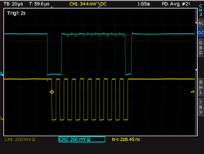
The captures below illustrates the I2C replies, when the 0x3F address was used with the read and write transfer modes for the PSoC function I2C_I2CMasterSendStart.
Midas Display - NACK to Read I2C Packet

The ninth bit (left MSB bit first) in the SCL clock train (yellow trace) in the above trace shows that the corresponding position in the SDA trace (blue trace) was high and therefore represents a negative acknowledgement (NACK) to the read command; the same bit position on the trace below has a low on the ninth bit (blue trace) represents an acknowledgement (ACK) to a write command.

Midas Display - ACK to Write I2C Packet

For further information, see Figures 6 and 7 in the TI document ‘Understanding the I2C Bus’ for waveforms relating to I2C ACK and NACK responses.

Code Changes
The code change mentioned in the above paragraph was implemented in the PSoC TestI2CAddress function located in 'main.c'. Other changes were made in main to suit the terminal program TeraTerm.

Testing Other Devices
To ensure the code change would work with other devices, two other I2C devices were tested; an Adafruit SI1145 light sensor and an INA219 current sensor

Test Setup - PSoC Development Board with SI1145 Sensor

Tera Term - I2C Address from SI1145 Sensor
Tera Term - I2C Address from SI1145 Sensor  

Test Setup - PSoC Development Board with INA219 Sensor

Tera Term - I2C Address from INA219 Sensor

Downloads and Disclaimer
The updated PSoC Creator project v1.1, for a PSoC4 device, can be downloaded as linked below. The original project is copyrighted and remains the property of Jörg Meier Software as noted in the project source.

I2CScan-v1_1.cywrk.Archive01.zip

Tuesday, 17 December 2024

PCB Artwork - Coaster (Dark Chocolate Imprint)

Introduction 
In this blog, the circuit board tool Altium Designer was used to create a circuit board (PCB) coaster with an imprint on the PCB resembling a dark chocolate (cocoa) molecule.

Example (Coffee) Cup Coasters
Prototype (Coffee) Cup Coasters

Finding a Suitable Source
Before the PCB design process could be started, a suitable molecule for the PCB imprint was found online. A representation of a molecule that was more uniformly shaped was chosen to suit the shape of the PCB. Such a specific layout may not be available without manipulating the molecule’s layout.

Dark Chocolate Molecule
(Courtesy biobeat.nigms.nih.gov)

The molecule in this post could have been caffeine, tea or several water molecules however for this post dark chocolate was chosen.

Creating the PCB
To begin creating the PCB artwork for the coaster in Altium, a circular arc on mechanical layer 1, with a 90 mm diameter was drawn. The 80 mm PCB diameter used in the previous coffee cup coaster was marginally too small however the overall PCB dimension should be adjusted on a project-by-project basis.

Coaster PCB Shape and Size

Next, the names of the individual chemicals were added as top copper layer strings. The font type sans serif was selected over serif for a modern appearance. Then the bonds between the chemical text were added to the PCB on the top overlay. Various placement and shuffling of top overlay line lengths and text were needed.

Coaster Top and Silk Layers

The next step was to duplicate the top copper layer strings. The layer properties of the copied strings were changed to the mechanical top solder layer and then placed over the top layer strings. This effectively removed the top solder mask exposing the PCB copper. Having a separate top solder layer allows for manipulation of the size and placement.

Coaster Top Solder and Silk Layers

Viewing the PCB using the Altium 3D feature yields the image below for the black solder mask.

Coaster in 3D
Coaster in 3D

PCB Export
The requirements of the desired PCB manufacturer were checked to prepare the PCB artwork for manufacturing. As the files for the PCB manufacturer are usually in the Gerber format, the export settings for the Gerbers should be verified with the manufacturer.

Manufacturing
As noted in other blogs, the appearance and cost of the manufactured PCB may vary based on Production settings. For the PCB in this post, a black solder mask is more expensive than a green solder mask, the latter being more common.

In this post, the PCB thickness was kept at 1.6 mm since this is usually the most cost-effective thickness, a lead-free HASL (Hot Air Solder Levelled) surface finish was chosen over a lead finish and the solder mask was produced in two separate colours, green and black, to exhibit the visual difference. Lastly, the PCB manufacturer's marking was specified on the PCB bottom side overlay.

Downloads
The Gerber file can be downloaded from the link below. The files should be checked before use.

For the Gerbers the Altium export settings here were followed.

Coaster Gerber Files