Showing posts with label altium. Show all posts

Tuesday, 17 December 2024

PCB Artwork - Coaster (Dark Chocolate Imprint)

Introduction 
In this blog, the circuit board tool Altium Designer was used to create a circuit board (PCB) coaster with an imprint on the PCB resembling a dark chocolate (cocoa) molecule.

Example (Coffee) Cup Coasters
Prototype (Coffee) Cup Coasters

Finding a Suitable Source
Before the PCB design process could be started, a suitable molecule for the PCB imprint was found online. A representation of a molecule that was more uniformly shaped was chosen to suit the shape of the PCB. Such a specific layout may not be available without manipulating the molecule’s layout.

Dark Chocolate Molecule
(Courtesy biobeat.nigms.nih.gov)

The molecule in this post could have been caffeine, tea or several water molecules however for this post dark chocolate was chosen.

Creating the PCB
To begin creating the PCB artwork for the coaster in Altium, a circular arc on mechanical layer 1, with a 90 mm diameter was drawn. The 80 mm PCB diameter used in the previous coffee cup coaster was marginally too small however the overall PCB dimension should be adjusted on a project-by-project basis.

Coaster PCB Shape and Size

Next, the names of the individual chemicals were added as top copper layer strings. The font type sans serif was selected over serif for a modern appearance. Then the bonds between the chemical text were added to the PCB on the top overlay. Various placement and shuffling of top overlay line lengths and text were needed.

Coaster Top and Silk Layers

The next step was to duplicate the top copper layer strings. The layer properties of the copied strings were changed to the mechanical top solder layer and then placed over the top layer strings. This effectively removed the top solder mask exposing the PCB copper. Having a separate top solder layer allows for manipulation of the size and placement.

Coaster Top Solder and Silk Layers

Viewing the PCB using the Altium 3D feature yields the image below for the black solder mask.

Coaster in 3D
Coaster in 3D

PCB Export
The requirements of the desired PCB manufacturer were checked to prepare the PCB artwork for manufacturing. As the files for the PCB manufacturer are usually in the Gerber format, the export settings for the Gerbers should be verified with the manufacturer.

Manufacturing
As noted in other blogs, the appearance and cost of the manufactured PCB may vary based on Production settings. For the PCB in this post, a black solder mask is more expensive than a green solder mask, the latter being more common.

In this post, the PCB thickness was kept at 1.6 mm since this is usually the most cost-effective thickness, a lead-free HASL (Hot Air Solder Levelled) surface finish was chosen over a lead finish and the solder mask was produced in two separate colours, green and black, to exhibit the visual difference. Lastly, the PCB manufacturer's marking was specified on the PCB bottom side overlay.

Downloads
The Gerber file can be downloaded from the link below. The files should be checked before use.

For the Gerbers the Altium export settings here were followed.

Coaster Gerber Files

Saturday, 18 February 2023

Altium Parameter Set Example

Introduction
This blog looks at other uses for the parameter set that is available when drafting in Altium Designers’ schematics.

Example of Altium Schematic with a Parameter Set Rule

Parameter Set Requirement
An engineering pack is commonly used to convey coherent and clear manufacturing information to a production company responsible for either printed circuit board (PCB) manufacture or assemblies (PCA). Some of the information or parameters contained in the engineering pack will vary vastly between companies.  For example, some components used on a circuit board may be specified to meet automotive or military grades. Other requirements may relate to the approval of component suppliers, the custom design of a component, or factory programmed to list a few. Whilst other companies may require components traceability if certain regulations or requirements such as PSE, IEC or ANSI are needed.

The component part number may usually contain sufficient detail for the requirements detailed in the above section however in other cases, additional product information may need to be shared with the manufacturing partner.

Parameter Set Use
This blog leans on the schematic parameter set available in newer releases of Altium Designer for providing additional component information to the production company. While pushing details into the parameter set may not be considered a clean integration compared to the Altium component database, changes can be made to a project without modification to the library. Details contained in the parameter set can still be reflected in reports such as the bill of materials (BOM). This solution may be helpful for projects where minimal business investment in the project is warranted but project control using a design tool is essential. 

Parameter Set Example
For the example in this blog, the Altium Designer project ‘Mini PC’ (courtesy Altium) will be used.

Altium Example Project - MiniPC

Target Schematic Page from Altium Example Project - MiniPC

Assume for the example in this blog that the jack and relay were hand populated. The circuit board loader in this example required documentation for components that required hand population.

Example Schematic Page with No Parameter Set

A blanket rule was placed over the power jack and relay schematic components.

Example Schematic Page with With Parameter Set

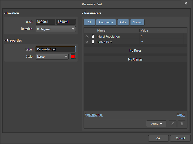
A parameter set rule was added to the blanket rule on the schematic, with the custom parameter ‘Hand Population'.

Example Altium Parameter Set

An additional custom parameter set for a ‘Listed Part’, was added to illustrate that multiple parameters could easily be added to the schematic as required.

Parameter Set in Bill of Materials
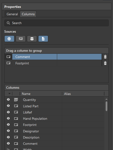
When generating the Bill of Materials (BOM) in Altium, details from the schematic parameter sets are available in the BOM Properties ‘columns’.

Altium BOM using Parameter Sets

Viewing the parameter set information in the BOM generated by Altium is possible by enabling the required parameter listed in the columns section of the BOM manager. This allows customisation of the various board fabrication or assembly houses.

Extract from Altium MiniPC Project with Parameter Sets

Pictured above is a portion of the generated BOM when the ‘Hand Population’ and ‘Listed Part’ parameter set entries were enabled.

For Altium projects that have several variants, components in schematics are likely to be controlled using the variants manager. Components are marked as fitted or not fitted. When a parameter set is used, the fitting of components with parameter sets in the BOM should be reviewed.

Wednesday, 7 October 2020

Altium Return Path Example Project

Summary
This blog provides an example Altium Designer (Altium) circuit board project which makes use of the ‘Return Path’ rule.

Altium reference material, such as Video content and documentation for configuring the 'Return Path' rule should also be reviewed when considering this feature.

Example
The Altium project for the Altera Cyclone II EP2C35F67C8 DB31.07 Daughter Board ‘DB31’ was used for the blog example. 

Altera Cyclone II EP2C35F67C8 DB31.07 Daughter Board
Altera Cyclone II EP2C35F67C8 DB31.07 Daughter Board by Altium

A single Printed Circuit Board (PCB) signal layer was used with a reference power plane to illustrate return paths.

PCB Layer Stackup
To achieve the desired board trace impedance, a PCB designer may liaise with a PCB fabrication company to define the layer stack, dielectrics, trace widths and for differential pairs the trace spacing.

As an example, the capture below shows typical information provided by a PCB fabrication company. The PCB was configured for impedance controlled differential pairs on external signal layers and single-ended internal layers.

Example PCB Manufacturer Trace Width Information

The types of material used for the PCB core and pre-preg depends on the capabilities of the PCB fabrication company and budget constraints.

Example PCB Manufacturer Layer Stackup

For the blog example using the DB31 project, the existing layer stack was retained. An arbitrary impedance of 55 R was selected for layer Mid-3 traces which was referenced to a single layer, Ground-5.

Example Project DB31 Layer Stackup
Example Project DB31 Layer Stackup and Controlled Impedance

Return Path Rule
As detailed in Altium documentation, the return path must be a fill, region or polygon which is unbroken. After configuring the impedance profile, a new ‘Return Path Rule’ was configured for layer Mid-3.

Altium Return Path Rule No Exclusions

The ‘Exclude Copper Vias’ checkbox was selected to ignore violations under the Altera FPGA as a result of vias. 

Altium Return Path Rule with Exclusions

Design Rule Check (DRC)
After performing a DRC on the original DB31 PCB, several violations required resolution.

DB31 Project PCB Net Antennae

Testing Return Path Violations
With the return path for Mid-2 signals being Ground-5, a cutout was inserted into the ground polygon at a location which resulted in a return path violation.

DB31 Project Cutout in Return Path Reference Plane

DB31 Project Signal Traces

After running a DRC, violations for Return Paths were shown for Mid-2.

DB31 Return Path Violations

Return Path Tolerances
Some factors not detailed in the Altium documentation are the tolerances of the 'Return Path' rule. Tolerances in this case refer to the amount of return path copper which can be removed from beneath the signal trace before a violation is raised by Altium Designer.

For the image shown below a cutout was placed in the return plane, Ground-5, which ran in parallel with the signal trace. This resulted in a violation.

Altium Return Path Violation Parallel Ground Cutout

In the capture below the edge of a rectangular cutout was placed in the return plane, Ground-5, which intersected with the signal trace.

Altium Return Path Violation Tolerance Ground Cutout

A return path violation was raised when the cutout encroached under half of the mid layer track. 

Altium Return Path Violation Tolerance Rectangular Cutout Measurement

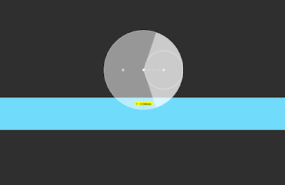
Next, a circular cutout was placed in the return plane which resulted in a violation at the position shown in the capture below.

Altium Return Path Violation Tolerance Circular Cutout Measurement

Final Thoughts
For circuit board designs containing features such as DDR memory, high-frequency differential pairs or high-speed inter-chip signals, utilising the 'return path' rule automates the previous manual checking required for return paths.

However, as with any tool, there are tolerances and limitations which would ideally be detailed by the manufacturer. The effects of polygon cutouts, the result of signal trace to return path coverage and details for return paths with coplanar impedance control are some trappings which may of interest to the PCB designer.

Acknowledgements
Thanks to Altium for the DB31 project which was used to illustrate the return path rule in this blog.

Downloads
The updated DB31 project used in the blog.


Friday, 25 September 2020

Altium PCB Art

Summary
This blog outlines techniques 
to produce PCB visual art utilising a Printed Circuit Board (PCB) design package with image editing software. Below is an example of a PCB, with exposed copper, portraying a Monkeyface.

Monkeyface as PCB Artwork

Preamble
During the pandemic lockdown, there was an opportunity to use a PCB design package, Altium Designer (Altium), for basic visual 'PCB' art. While Altium can be used independently to create visual art, utilising a free image editing package such as GIMP, Inkscape or a commercial package such as Photoshop or Corel will assist with altering images.

The image editing methods described in this blog are experimental; alternative techniques are welcomed!

Software Alternatives
Free PCB software design packages which include KiCad, Design Spark and PCBWeb are capable of creating similar PCB art.

Source Material
Source material, such as an image or a DXF file, are usually required with a PCB design package. Monochrome images can ordinarily be pasted directly into Altium however loss in greyscale images can occur with lighter tones. Colour images require conversion to black and white. Images can be converted into a DXF format and imported into Altium.

Example 1: Colour to Monochrome - Cloud Sun
All credit to the creator of the artwork
Sushant Wadte, for the example image below.

Colour images are changed into monochrome using various methods. The subsequent method, using filters in Inkscape, produces reasonable results in images with large objects.

Cartoon Sun Cloud
Cartoon Sun Cloud - Courtesy PNGItem. Creator - Sushant Wadte

Using the 'Greyscale' filter in Inkscape, the colour image was converted to monochrome. The colour channels and lightness were adjusted to improve the monochrome image.

Inkscape Greyscale Filter - Cartoon Sun Cloud

For importing into Altium, the monochrome image background was changed to white and all other features were converted to black.

Inkscape Black and White Cartoon Sun Cloud

Filling the cloud and sun rays with black was performed using Inkscape's fill bounded areas tool. The image background was filled with white.

The converted image was saved as a BMP and PNG file.

Altium Script (Alternative Import Method)
The Altium script PCBLogoCreator was used to convert the bitmap image into a representation in tracks.

Inkscape Dialog Box Running PCBLogoCreator Script
Altium Dialog Box Running PCBLogoCreator Script

Running the Altium script on the black and white image for a PCB, yielded the resulting image shown below.

Altium Script Converted Cartoon Sun Cloud
Altium Script Converted Cartoon Sun Cloud 

The image converted by the script was useable, although there are two points to highlight. 
Firstly, converting the image results in hundreds of tracks which can load up the CPU when moving the tracks. Secondly, the tracks cannot be selected and converted to a polygon or region.

Altium Script Conversion Lines Cartoon Sun Cloud

Placing Sun Cloud PNG Into Altium
The saved PNG image can make its way into Altium using two methods. One method is to cut and paste into an Altium PCB. Another method is to use the menu command, Place Object.

The same black and white image in the previous section was pasted into Altium onto the top layer (copper).


Altium Pasted PNG Cartoon Sun Cloud

Selecting the cloud on the pasted image shows that the process of pasting into Altium converts the image dark areas to regions.

Object Tweaks
The image was initially pasted on the PCB top layer (copper) although it is possible to paste onto other layers such as the top overlay (silkscreen).

Altium 3D Top Silk Unmodified Cartoon Sun Cloud

The cloud was changed to top layer silk and the sun and rays left as copper. To change the cloud from top copper to top silk, the cloud region was modified.

Altium Cloud Region Selection

The Properties (legacy PCB Inspector) was opened to change the region from top copper to top silk. 

Altium Region Layer Change

With the cloud changed to silk, the remaining objects required removal of the solder mask (green coating).

Altium Top Silk Cloud Region
Altium Top Silk Cloud Region 

To alter the solder mask of the remaining objects, each region was selected. The region 'Properties' (legacy PCB Inspector) was opened and the 'Solder Mask' rule changed.

Altium Object Solder Mask Expansion
Altium Object Solder Mask Expansion

The 'Solder Mask Expansion' setting was set to 'Manual'. Having a 'Solder Mask Expansion' value may be required depending on the capabilities of the PCB manufacturing house.

The resulting capture of the PCB, in 3D, shows the changes.

Altium 3D Modified Cartoon Sun Cloud

PCB Shape - Cloud Sun
The PCB outline was defined using tracks on Mechanical 1 layer as this layer is commonly used to define the shape of the PCB.

PCB Finish - Cloud Sun
For the example PCB displayed above, a green solder mask and ENIG copper finish (gold) were used. Some alternative solder mask colours are red, blue, yellow, white, black and purple. The copper can be left raw to discolour due to oxidisation or coated with a finish such as lead-free solder, tin, silver or gold.


Example 2: Colour to Monochrome - Monkey
Converting the monkey image for use as art in Altium used a similar method to the first example.

Monkey Face - Courtesy free.clipArtOf.com
Monkey Face - Courtesy Free.ClipArtof.com

Some additional work was required to remove the colour and gradients. Firstly, the Greyscale filter in Inkscape was used to convert the image to monochrome.


Inkscape Greyscale Filter - Cartoon Monkey Face

Using the 'Fill Bounded Areas' tool in Inkscape, the areas with colour gradients were filled with white. There was a gradient (shadow) below the face which was also filled with white. 

Inkscape Monkey Face Monochrome No Shading

Visible lines in the image may be imported by Altium and therefore these lines were removed. Using Inkscape's 'Brilliance' filter, the Brightness and Lightness settings were adjusted to remove the lines. Producing the desired results with this tool can take some tweaking.

Inkscape Brilliance Filter - Cartoon Monkey Face

Monkey Black and White
The cut and paste results in Altium are significantly improved when all colours are black. The 'Fill Bounded Areas' tool was used to ensure all regions were converted to black.

Inkscape Cartoon Monkey Face All Black Lines

The image in Inkscape was exported as a PNG ready for import into Altium.

Placing Cartoon Monkey PNG Into Altium
Using the Place Object command in Altium, the Cartoon Monkey was added to a new blank PCB on the top copper layer.


Altium Cartoon Monkey Face Import

Object Tweaks
For the Monkey design, all copper areas were changed to show exposed copper. The Solder Mask expansion changed to manual for all the copper areas.

Altium Cartoon Monkey Face Copper Selected

Viewing in 3D showed that the solder mask was removed from the copper.

Altium Cartoon Monkey Face Exposed Copper

PCB Shape - Monkey
The PCB outline was defined using arcs around the Monkey head. These arcs were drawn on the Mechanical 1 layer as shown in the image below.

Altium Cartoon Monkey Face Mech1 Layer

Setting the PCB shape was performed with the Mechanical 1 Layer arcs selected then using the Altium command Define PCB from Selected Objects.

Altium Cartoon Monkey Face Board Cutout

Final Touches - Monkey
Holes were made for the Monkey eyes using two pads having a 3.8 mm holes.

Altium Cartoon Monkey Face Eye Holes

Pictured below is the final PCB in 3D with exposed copper and holes for the eyes.

Altium Cartoon Monkey Face Final

PCB Finish - Monkey
A black solder mask and ENIG copper finish (gold) were used for the PCB finish.

Example 2: Alternative Monkey
To achieve a PCB design similar to the image shown at the beginning of the blog, the black and white image required inversion. At the previous step 'Monkey Black and White', the image was inverted.

Monkey Head as PCB Artwork

The Inversion Filter in Inkscape performed the conversion.

Inkscape Invert Cartoon Monkey Face

Adding a Border
After the Inversion, the image boundaries became the four extremities of the Monkeyface. Adding a black background using Inkscape assisted when importing the image into Altium.

Inkscape Monkey Face Inverted with Border

With a black rectangle drawn in Inkscape, the inside area was filled with black. 

Inkscape Monkey Face Inverted with Background

Placing Cartoon Monkey PNG Into Altium
Below is the PCB capture after using the Place Object command in Altium.

Altium Cartoon Monkey Face Alternate Import

Object Tweaks
For the alternate Monkey design, the internal copper areas were changed to exposed copper.

Altium Cartoon Monkey Face Alternate Exposed Copper

PCB Shape - Monkey
The PCB outline comprised of two parts, a board cutout and the PCB shape on the Mechanical 1 layer. Firstly, the remaining copper region outside the Monkeyface was selected then changed into a 'Board Cutout'.


Altium Copper Region to Board Cutout

Viewing in 2D shows the board cutout.

Altium Cartoon Monkey Face 2D Cutout

Secondly, a Mechanical 1 Layer was added onto the PCB to define the physical PCB size. The Mechanical 1 Layer tracks were selected and the PCB shape was defined from the selected objects.

Altium Cartoon Monkey Face Alternate Mech 1 Layer

Viewing the PCB in Altium 3D.

Altium Cartoon Monkey Face Alternate Final

Alternative PCB Shapes
Inkscape provides a tool called Trace Outline which can be useful when the shape of the PCB must be marginally different to the image shape. A modified outline can be imported into Altium as a separate object which would then be used to define the outline of the PCB.

Inkscape Monkey Face Trace Outline

Final Thoughts
The methods described in this blog can be used independently or partnered with electronic circuits to create visual PCB art. 

It should be noted that the placement of copper as art is not limited to either side of the PCB but internal copper layers also. Using only internal copper and a thinner PCB (1 mm or less) produces near translucent effects with the suitable backlighting.