Showing posts with label PCB. Show all posts

Sunday, 19 January 2025

Crosstalk Test PCB (Educational)

Introduction 
The Printed Circuit Board (PCB) design in this post was inspired by the well-known signal integrity educator, and professor, Eric Bogatin. The board design was based on content shown in a YouTube video created to demonstrate crosstalk.

Crosstalk PCB 3D
Crosstalk PCB 3D

Why This Design?
Following on from the PCB trace-to-trace crosstalk content created by YouTuber Robert Feranec with guest Eric Bogatin, I wanted to design a simple educational board that would allow crosstalk measurements to be made on a PCB and tested when passive elements were introduced into PCB traces. Crosstalk measurements with series and parallel resistor signal path terminations are common in many PCB designs and this PCB design was designed specifically for series terminations.

Circuit Board Design
A regular 1.6 mm board (FR4) double-sided PCB was chosen for the design. For the copper layers, a reference plane was placed on one side of the PCB and impedance-controlled traces were placed on the opposite side. Using PCB design software tools, the configuration of the trace impedance (width) was tuned for around 50 R impedance giving a 2.8 mm trace width. The 50 R impedance is given a tolerance of + 10 % as this is the standard tolerance for PCB fabrication houses in the local region.

Altium Impedance Profile 50 R for Crosstalk PCB
Altium Impedance Profile 50 R for Crosstalk PCB 

As a crosstalk PCB design features two signal traces, the spacing between the traces was set at less than a track width to ensure ample signal coupling between traces.

Crosstalk PCB 2D
Crosstalk PCB 2D

As the series element, a resistor footprint was included in one of the PCB test traces.

Crosstalk PCB Resistor Linked

This footprint on the PCB provided an option to test with different resistor values and then measure the effects with suitable test equipment. A pulse generator with a fast edge and an oscilloscope are required.

The first setup on the test PCB has the series resistor on the same layer as the signal trace and the second test setup has the resistor on the opposite side to the trace, connected through vias.

Board Build and Initial Testing
For the board assembly, the Molex SMA connectors were fitted. The Molex part number is 
0732512120. For the validation test, the resistors on the PCB were replaced with solder shorts.

During testing, the trace with the series resistor is referred to as the aggressor and the nearby sensing trace, is the victim. Further details relating to this setup and a further explanation can be found in the aforementioned video content with Robert Feranec.
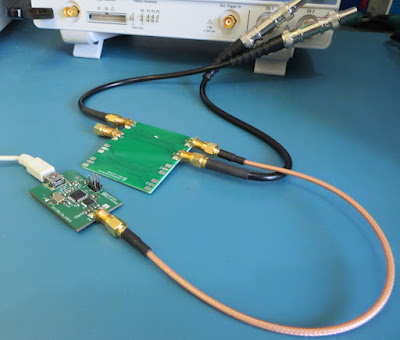
First Test Setup with Crosstalk PCB and Pulse Generator

For validation, measurements were taken using an oscilloscope with a bandwidth of less than 500 MHz and a simple pulse generator (Microchip version) designed in a previous blog.

Pulse Generator Frequency

Pulse Generator Rise Time

With the pulse generator providing the 1.4 ns rising edge signal into the aggressor trace (CH2 blue trace), the connector at the near end of the victim trace (CH1 yellow trace) was connected to the oscilloscope.

Near End Crosstalk PCB Measurements

For a second measurement, the two ends of the victim trace were connected to oscilloscope. When the pulse was applied to the aggressor,  the signal entering and then reflecting (near and far end) was measurable.

Near and Far End Crosstalk PCB Measurements


Summary
This short post introduced a printed circuit board for testing the behaviour of signals relating to crosstalk measurements. The option to use a series resistive element was included but not tested in this post. 

The PCB Gerber files are downloadable using the link below for those who prefer to build the board and perform testing at home, school or in the lab. The Gerber files use the format as defined on this page.

Crosstalk PCB Gerber Files


Tuesday, 17 December 2024

PCB Artwork - Coaster (Dark Chocolate Imprint)

Introduction 
In this blog, the circuit board tool Altium Designer was used to create a circuit board (PCB) coaster with an imprint on the PCB resembling a dark chocolate (cocoa) molecule.

Example (Coffee) Cup Coasters
Prototype (Coffee) Cup Coasters

Finding a Suitable Source
Before the PCB design process could be started, a suitable molecule for the PCB imprint was found online. A representation of a molecule that was more uniformly shaped was chosen to suit the shape of the PCB. Such a specific layout may not be available without manipulating the molecule’s layout.

Dark Chocolate Molecule
(Courtesy biobeat.nigms.nih.gov)

The molecule in this post could have been caffeine, tea or several water molecules however for this post dark chocolate was chosen.

Creating the PCB
To begin creating the PCB artwork for the coaster in Altium, a circular arc on mechanical layer 1, with a 90 mm diameter was drawn. The 80 mm PCB diameter used in the previous coffee cup coaster was marginally too small however the overall PCB dimension should be adjusted on a project-by-project basis.

Coaster PCB Shape and Size

Next, the names of the individual chemicals were added as top copper layer strings. The font type sans serif was selected over serif for a modern appearance. Then the bonds between the chemical text were added to the PCB on the top overlay. Various placement and shuffling of top overlay line lengths and text were needed.

Coaster Top and Silk Layers

The next step was to duplicate the top copper layer strings. The layer properties of the copied strings were changed to the mechanical top solder layer and then placed over the top layer strings. This effectively removed the top solder mask exposing the PCB copper. Having a separate top solder layer allows for manipulation of the size and placement.

Coaster Top Solder and Silk Layers

Viewing the PCB using the Altium 3D feature yields the image below for the black solder mask.

Coaster in 3D
Coaster in 3D

PCB Export
The requirements of the desired PCB manufacturer were checked to prepare the PCB artwork for manufacturing. As the files for the PCB manufacturer are usually in the Gerber format, the export settings for the Gerbers should be verified with the manufacturer.

Manufacturing
As noted in other blogs, the appearance and cost of the manufactured PCB may vary based on Production settings. For the PCB in this post, a black solder mask is more expensive than a green solder mask, the latter being more common.

In this post, the PCB thickness was kept at 1.6 mm since this is usually the most cost-effective thickness, a lead-free HASL (Hot Air Solder Levelled) surface finish was chosen over a lead finish and the solder mask was produced in two separate colours, green and black, to exhibit the visual difference. Lastly, the PCB manufacturer's marking was specified on the PCB bottom side overlay.

Downloads
The Gerber file can be downloaded from the link below. The files should be checked before use.

For the Gerbers the Altium export settings here were followed.

Coaster Gerber Files

Wednesday, 29 May 2024

PCB Artwork - Model Rocket

Introduction 
In this blog the circuit board tool, Altium Designer, was used to create circuit board artwork in the form of a model rocket keyring. The recent prototype of the Wi-Fi rocket launcher post inspired this blog.

Model Rocket Keyring

PCB Artwork
To start the project, a black-and-white image of the rocket keyring was downloaded from a suitable website. An image called SpaceShipOne was downloaded from CleanPNG (all credits).

Scaled Rocket Image (Courtesy CleanPNG)

The original image was scaled by 25% before importing into Altium. Shown below is the result of the import. As can be seen by the imported image, the image did not produce solid lines which was required for the keyring.

Imported Rocket Image

Rather than manipulating the PNG file for an improved import result within Altium, the outline of the imported PNG was drawn over with circuit board tracks (traces). For simple shapes such as the rocket, using Altium is relatively easy however many other packages could be used to achieve the same drawing.

Drafting Rocket Primitives

The image below shows the imported image and the hand-drawn image side by side. Minor changes can be noticed on the rocket fins compared to the original image.

Comparison of Drawn and Imported Rocket Designs
Comparison of Hand Drawn and Imported Rocket Designs

One item not included in the circuit board file was the board outline. This is commonly added on a mechanical layer but this was not added to the design. It has been noted that many other free software tools are being used to create circuit board artwork. Therefore, with the alternative software in mind, the board manufacturer was asked to add a circuit board outline.

Manufacturing

For the circuit board manufacturing, the company JLCPCB was used. JLC included a board outline 0.1 mm from the circuit board trace. The final product is shown below.

Model Rocket Keyring


Download

For anyone interested in producing a keyring, the Gerber file pack is available below. A board outline should be spaced at least 0.1 mm from the outermost circuit board traces.

Rocket Keyring Gerbers


Monday, 25 March 2024

PCB Artwork - Coffee Cup Coaster

Introduction 

In a previous blog, the circuit board drafting tool Altium Designer was used to create circuit board (PCB) artwork. In this blog, a coffee cup coaster was created using the same technique.

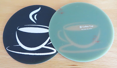
Coffee Cup Holder Front and Back

Removing Colour and Changing the File Format

To begin, select the desired clipart image from your preferred site, such as the image used in this post - a coffee cup. All credit to the original designer and provider of the coffee cup.

Coffee Cup Clipart (Credit Clip Library)

Import the image into an editing tool such as GIMP, Photoshop, or a free online editor. Remove any colour from the image (black and white) to prepare it for use on the PCB. Increase the thickness of the image as needed to ensure ease of production.
After the image editing is complete, save the updated image in a PNG format. This format allows for easy copying and pasting into Altium Designer.

Creating the PCB

To begin creating the PCB artwork for our coffee cup coaster, a circular arc (mechanical layer 1) with an 80 mm diameter to the PCB. This arc defined the board shape and should be larger than the image. An 80 mm diameter suits cups, a 100 mm to 120 mm diameter would suits most mugs.

Coaster PCB Shape and Size

Next, the PNG file contents were copied and pasted into Altium Designer. The imported image is represented by various regions which can be moved as needed.

For the coffee cup, the top copper layer was adjusted using the Properties dialogue box.

Manual Solder Mask Expansion Setting in Altium

To ensure a minimum distance between the solder mask and the copper layer, the solder mask expansion of the copper region was manually reduced to zero using the Properties dialog.

The steam seen above the coffee image was changed to a top-layer silk screen using the same Properties dialog in Altium.

Coffee Cup Coaster in Altium 2D

PCB Export

To prepare the PCB artwork for manufacturing, the file format (Gerber) needs to meet the requirements of the selected PCB supplier. The format may vary depending on the manufacturer and is usually listed on their website. In this post, the JLCPCB supplier was utilised to manufacture the PCB.

Manufacturing

The final appearance and cost of the coaster can vary greatly based on various factors. These factors include the thickness of the circuit board material, surface finish, solder mask and silkscreen colour.
In this post, the board thickness was maintained at 1.6 mm, the surface finish was lead-free HASL (Hot Air Solder Levelled), the solder mask was changed to black on the top side only and the silk screen was kept as white.

Coffee Cup Coaster in Altium 3D

Final Product

Pictured below is an image of the board as supplied by the manufacturer.

Coffee Cup Coaster on the Bench

Due to lighting the contract between the silver surface and the white silkscreen is not captured. To increase the longevity of the coaster, a clear epoxy or a hard-wearing lacquer could be applied. This will prevent the HASL coating from becoming tarnished over time.

Coaster in Use
Coaster in Use

Thursday, 31 August 2023

PCB Mouse Bites and Board Traces

Introduction 
This blog shows testing of
circuit board mouse bites that have copper traces passing through them. The breaking strength of the mouse bite was also measured during testing.

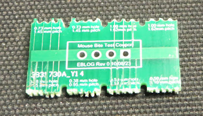
Mouse Bite Test Boards

Mouse Bites
The use of mouse bites with circuit boards can be as varied as the application however, some common examples of applications include board panelisation, tooling strips, test coupons, in-circuit testing or breakaway boards. This blog’s focus is on small breakaway boards commonly used in embedded programming or development boards where traces are routed through the mouse bites.

SparkFun published a white paper in 2022 (Author, Nick Poole) that illustrated testing of various mouse bite combinations. The paper from SparkFun serves as a good reference for designer as it details the combinations and the force required to break the board under test (mouse bite).

This blog performs similar tests to those conducted by SparkFun however, the intent was also to see the effect of circuit board traces after breaking the mouse bites.

Test Board
A circuit board was created with four mouse bite configurations. The drill hole sizes varied between 0.38 mm to 1.00 mm. The pitch between holes was adjusted to suit the drill size and test boards.

Test Board for Mouse Bites

Between the holes of the mouse bites, traces were routed either externally (top and bottom) or internally traces (two mid-layers). This created eight combinations of trace and mouse bites for testing.

3D View of Test Board for Mouse Bites

Measurements
For each mouse bite break measurement, a simple setup containing an attachment to the test board and connecting wire to a digital scale was used.

Mounted Test Board

Measurement Tool
Measurement Tool

Results
The table below lists the test number against the mouse bite drill size and pitch combination. 

Mouse Bite Configurations

As seen in the chart below, there was little difference in test results between the various mouse bite configurations and lifted board traces. External board traces on average lifted on the opposite side of the circuit board. Any lifted traces were considered damaged. No internal traces were seen to be damaged.

Type vs Listed Traces After Testing

The chart beneath shows the average measurement (kg) required to break the mouse bite boards. A notable difference in the last two tests was expected because of the larger mouse bite holes meaning less circuit board material.

Measurements for Breaking Mouse Bites
Type vs Measurements for Breaking Mouse Bites

The edge view of the main board in the image below shows the different breakage patterns.

Circuit Board Edge with Mouse Bites Removed

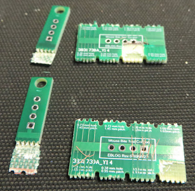
During two measurements, the test board broke cleanly except for one layer that lifted and tore away from the main board; as shown in the picture below.

Damaged Test Boards
Damaged Test Boards

Summary
The results in this blog with the specific test board indicate that internal traces experienced fewer issues with lifted traces. Other combinations of routing such as using a single side for external traces will likely be effective.

Mouse Bite Test Piece

For designs only requiring mouse bites in a circuit board design, most hole-pitch configurations are useable although the overall design should be reviewed as part of Engineering practices.

Sunday, 20 February 2022

Example Lids as Circuit Boards (PCB) Part 2

Summary
This short blog
follows on from the previous blog listing some drawings for lids/plates that were replaced with circuit boards.

Hammond 1455N1601 with Press Fit Panel

Circuit Boards Lids
While the previous blog used a clearance of at least 0.1 mm per edge, some of the new lids used an interference fit. Board dimensions should be validated to suit each design.

Again for verification, the Altium Designer files were saved as STEP files, converted to STL files then 3D printed before manufactured.

The DXF files below were generated using the Export feature in Altium Designer. The listed DXF files can be imported into an Altium PCB project using measurements in millimetres.

PCB Lid DXF for NUB505017

Tuesday, 30 November 2021

Example Lids as Circuit Boards (PCB)

Summary
This short blog
lists a handful of drawings for lids/plates of instrument cases that were replaced with circuit boards.

Example Project using 3D Printed PCB Panel (Multicomp MC002212)

Front Plates as Circuit Boards
The lid or plate on an instrument case is commonly manufactured as a plastic such as ABS, diecast aluminium or steel. These can be readily be replaced with a circuit board. Some of the benefits and drawbacks of using the circuit board are listed below.

  1. Customised appearance and colour in a single process (no separate decal or printing),
  2. Electronics can be added to the circuit board providing additional real estate,
  3. Circuit board may have benefits for EMC compared to standard plastic items (not metal screened),
  4. Minimal to no machining or manufacturing work for the circuit board,
  5. Iterating circuit board designs may end up faster than updating CAD for metal lids or plates,
  6. Plastic or metal lid or plate becomes waste or at best recycled if not used,
  7. Reworking a circuit board for mechanical purposes is not always possible,
  8. Circuit boards usually require more processes to recycle.

Example Lids as Circuit Boards
Shown below is a generic plastic enclosure called a jiffy box with a 3D plastic lids designed in Altium. 

A clearance of at least 0.1 mm per edge was chosen however the clearance should be adjusted as required due to variations in manufacturing.

Jiffy Box with 3D Printed PCB Plate

 
For verification, the Altium Designer files were saved as STEP files, converted to STL files then 3D printed. The files below were generated as DXF files using the Export feature in Altium designer. These DXF files can be imported into an Altium PCB, using a measurement in millimeters with the board shape defined on Mechanical-1.

PCB Lid DXF for Jiffy Box UB3


PCB Lid for Hammond (Eddystone) 27969PS


PCB Lid for Multicomp (Element14) MC002212