Showing posts with label Rocket. Show all posts

Wednesday, 29 May 2024

PCB Artwork - Model Rocket

Introduction 
In this blog the circuit board tool, Altium Designer, was used to create circuit board artwork in the form of a model rocket keyring. The recent prototype of the Wi-Fi rocket launcher post inspired this blog.

Model Rocket Keyring

PCB Artwork
To start the project, a black-and-white image of the rocket keyring was downloaded from a suitable website. An image called SpaceShipOne was downloaded from CleanPNG (all credits).

Scaled Rocket Image (Courtesy CleanPNG)

The original image was scaled by 25% before importing into Altium. Shown below is the result of the import. As can be seen by the imported image, the image did not produce solid lines which was required for the keyring.

Imported Rocket Image

Rather than manipulating the PNG file for an improved import result within Altium, the outline of the imported PNG was drawn over with circuit board tracks (traces). For simple shapes such as the rocket, using Altium is relatively easy however many other packages could be used to achieve the same drawing.

Drafting Rocket Primitives

The image below shows the imported image and the hand-drawn image side by side. Minor changes can be noticed on the rocket fins compared to the original image.

Comparison of Drawn and Imported Rocket Designs
Comparison of Hand Drawn and Imported Rocket Designs

One item not included in the circuit board file was the board outline. This is commonly added on a mechanical layer but this was not added to the design. It has been noted that many other free software tools are being used to create circuit board artwork. Therefore, with the alternative software in mind, the board manufacturer was asked to add a circuit board outline.

Manufacturing

For the circuit board manufacturing, the company JLCPCB was used. JLC included a board outline 0.1 mm from the circuit board trace. The final product is shown below.

Model Rocket Keyring


Download

For anyone interested in producing a keyring, the Gerber file pack is available below. A board outline should be spaced at least 0.1 mm from the outermost circuit board traces.

Rocket Keyring Gerbers


Sunday, 28 April 2024

Model Rocket Launcher WiFi ESP8266 Part 3

Introduction 
This blog continues from Part 2 of the ‘Wi-Fi-controlled rocket launcher’. In this blog, the software changes to suit the ESP8266 are mentioned. Additionally, a mechanical 'proof of concept' for the rocket launcher is shown using a 3D-printed case.

Bench Test of Rocket Launcher

Code Change Summary
In the earlier version of the model rocket launcher design, a PSoC microcontroller with Bluetooth was selected for communications. When moving to the ESP8266, the Bluetooth communications interface was changed to a Wi-Fi interface. Using a Wi-Fi interface simplified the design when compared to developing in Android Studio.

To support a broader audience using the ESP8266, it was decided to perform software development using the Arduino platform.

/** *****************************************************************************
* @file   main.c
* @version 1.0b
* @date 10/02/2024
* @brief
* 01/03/2023  Moved code from original PSoC version into Arduino
* 13/01/2024  Changed code operation, updated launch state machine
* 24/01/2024  Client connection issues noted during testing
* 10/02/2024  Code cleanup. Changed deprecated server.available() to server.accept()
****************************************************************************** */

#if !defined(ESP8266)
  #error For ESP8266. Check Tools->Board setting
#endif

/*_TIMERINTERRUPT_LOGLEVEL_ from 0 to 4 */
#define TIMER_INTERRUPT_DEBUG         1
#define _TIMERINTERRUPT_LOGLEVEL_     1
#define ENABLE_DEBUG_PRINTS           true

Most parts of the original code from the PSoC, including the launcher state machine, were either updated or rewritten. Code changes were needed for the ESP and targeted toward proper encapsulation.

ITimer.attachInterruptInterval(TIMER_INTERVAL_MS * 1000,TimerHandler);  /* 10 ms system timer */
      

Snippets and libraries from the Arduino community were included in the new launcher code. Specifically, credit goes to Khoi Hoang for Timer Interrupt examples and Martyn Currey for ESP Wi-Fi implementation.

How Software Was Developed
The code was developed using the Arduino IDE. Initial testing for the ESP code was performed using a Windows laptop for the Wi-Fi connection primarily to test the webpage interface. Testing subsequently progress to  an Android phone.

Shown in the image below is the first rocket launcher web page. Additional information such as battery voltage and launch state may be included on the web page in later updates.

Rocket Launcher Webpage
 

Launcher Case
After reviewing the previous enclosure and cost, it was decided to design a 3D-printable enclosure to house a small lead acid battery and a control board. The lead acid battery is only temporary and will be changed to an 18650-cell(s) capable of a high-discharge current.

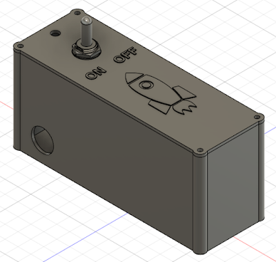
For the 3D-printed case, two mechanical parts were drafted in Fusion 360. These parts comprised of a base and a lid as pictured below.

Rocket Launcher Case (Fusion 360)
 

Launcher Hardware Assembly
With the ESP code allowing the desired launch operation, the circuit board, wiring and battery were assembled and added to the 3D-printed case.

Rocket Launcher Test Assembly

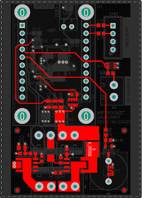
During the assembly, it was noted that the pluggable circuit board headers, although simple to install and use, were expensive and consumed space. On the subsequent revision of the board, as displayed below, the pluggable headers were replaced with through-hole solder pads that suit a larger gauge wire.

Updated Launcher Board

Additionally, the toggle switch used for controlling the power was salvaged from another project. There are no manufacturer markings on the switch to generate a Bill of Materials. More clearance was added around the toggle switch body to suit other types of toggle switches such as the model shown below.

Standard Toggle Switch

Complete Test Assembly
For a bench test, a lamp was used as the igniter as pictured below. A short video of the operational launcher is exampled in the video.


The next post will feature the updated launcher circuit board and field testing.

Sunday, 22 October 2023

Model Rocket Launcher WiFi ESP8266 Part 2

Introduction 
This blog continues from Part 1 of the WiFi-controlled rocket launcher. In this short post, load testing was performed on the igniter's power supply and the output drivers.

WiFi Rocket Launcher Blank PCB

Power Supply
The DC-DC converter, Texas Instruments part LMR50410, was tested for switch ON voltage threshold and response. Since the converter powers an ESP module and output drivers for the igniter, the load current test was set for 300 mA.

Power Supply Portion of WiFi Rocket Launcher
Power Supply Portion of Rocket Launcher

An external power supply was connected to the launcher board. The voltage was increased in increments of 100 mV until the converter activated. For this board, the threshold was 4.1 V. The output switch ON waveform is shown below.

Rocket Launcher Power Supply Supply Turn ON

A resistive load resulting in 330 mA was connected to the 3.3 V supply for testing. The output voltage dropped from 3.3 V to 3.28 V when the load was connected.

Rocket Launcher Power Supply Supply Transient Response

The transient response for the power supply was measured for a 50 % load change. Captured in the image above is the response showing a recovery time of less than 200 ns for the supply voltage to settle back to 50 mV.

Output Drivers
The output driver circuit design had been established from the previous version of the launcher circuit board, which meant the operation was already known.

Rocket Launcher Output Driver Load Testing

To test the output drivers on this board, a 5 Ω resistive load was used. The two output drivers were powered with 12 V to simulate the primary power source. Using the 3.3 V from the converter, the two drivers were activated.
V(supply) = 11.92 at drivers no load, V(supply) reduced 11.79 V with approximately 2.3 A load current because of cable losses.

Measurements were taken with 2.3 A of load current
V(load) = 11.19 V
V(diode) = 401 mV
V(high side driver) = 102 mV
V(low end driver) = 124 mV

In par
t 3, the code for the rocket launcher will be started in Arduino IDE.

Saturday, 24 June 2023

Model Rocket Launcher WiFi ESP8266

Introduction
This blog follows the redesign and development of a model rocket launcher controller that features WiFi communications to control the launch process. This design uses an ESP-based microcontroller module. The Arduino platform was chosen for code development.

Rocket Launcher 3D Model

Redesign
To control the launch in the previous model rocket launcher design, Bluetooth communications were used between a PSoC microcontroller and an Android phone. The interface was changed to WiFi to remove the need for developing a phone application. Controlling a rocket launch through WiFi would be independent of a phone or computer operating system.

WiFi Module
For the launcher redesign, an off-the-shelf ESP module capable of WiFi was chosen from Adafruit. The ESP module was chosen for a few reasons. Firstly, the module’s price was relatively low (USD 10). The module was readily available compared to other dedicated microcontrollers. Lastly, using an ESP module meant that the rocket launcher design could be migrated more easily to other ESP devices.

Adafruit Huzzah ID 2471 (Courtesy Adafruit)

Reused Design
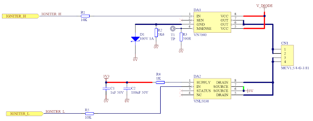
The same section of circuit responsible for driving the rocket engine igniter was taken from the previous design. This section consisted of high (VN7040) and low-side (VNL5030) switching drivers (ST Microelectronics).

Rocket Launcher Igniter Drive Circuit

Circuit Updates
To begin the schematic update process, the ESP module was created in the schematic libraries. The new part replaced the previous PSoC microcontroller and associated circuitry.

The Altium PCB model was downloaded from the website SnapEDA.

Capture of Adafruit Huzzah PCB Footprint from SnapEDA

Schematic Updates
On the ESP module schematic page, the power supply connections and ST driver control signals were mapped to the ESP.

Rocket Launcher - Huzzah Circuit Connections

Audible notification of an impending launch was retained using the buzzer. Connections were mapped to the ESP.

Rocket Launcher - Buzzer


The display (LCD) was infrequently used in the previous design so it was removed and replaced with an LED.

The launch button input to the ESP module was retained for testing purposes.

Rocket Launcher - Optional Launch Button

Connections were made to ESP module pins that had no special functions.
 
Output Drivers

Schematic changes were made to the ST output driver’s power supply. This was required to match the ESP module’s DC 3.3 V supply voltage. The feedback monitoring from the ST drivers was removed from the design because of the reliable performance of the ST drivers.

Power Supply
A DC-DC step-down converter was retained for the power supply. Texas Instruments part LMR50410 featuring an integrated diode was selected to replace the previous DC-DC converter.

Another benefit of the DC-DC converter is its operating voltage which is wider than the ESP modules linear regulator (LDO). The LDO has a maximum rated input voltage of DC 6 V. This voltage does not suit all battery chemistry types.

Rocket Launcher - Power Supply

Battery voltage monitoring using the ADC on the ESP through a resistor divider was kept for experimentation and possible future use.

Circuit Board
There were no caveats defined for the shape of the circuit board (PCB). The placement of components drove the PCB shape. Minimal design constraints for the PCB meant that the PCB was set up for components on both sides.

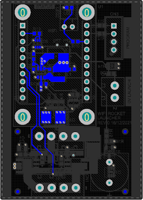
The capture below shows the PCB top layer with the ESP module, power supply underneath the ESP module, buzzer and optional screw terminals. To fit the power supply beneath the ESP module, pluggable headers were utilised to space the ESP module off the board.

Rocket Launcher PCB - Top Layer

The next capture below shows the PCB bottom layer containing the output switching drivers and related components.

Rocket Launcher PCB - Bottom Layer

Four PCB layers were used for the launcher board stack-up. Captures of the two internal power planes have not been shown.

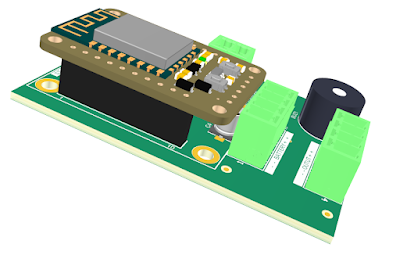
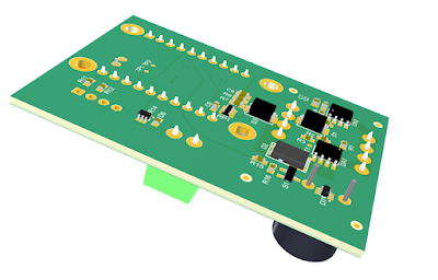
After component placement and routing, the board size reached a comfortable size of 62 x 44 mm. On the longest PCB axis, a set of 3 mm strips were added to suit mounting in an enclosure. Pictured below is a 3D side and rear view of the board.

Rocket Launcher - 3D Side View
Rocket Launcher - 3D Rear View

In part 2 of the launcher blog, the PCB construction and initial testing will be performed.

Saturday, 30 January 2021

PCB Prototype to Manufacture Example (Bluetooth Model Rocket)

Summary
Illustrated in this blog are modifications to the prototype Bluetooth Model Rocket Launcher (Launcher) carrier Circuit Board (PCB) with a view to manufacturing. This blog uses a prototype board to highlight facets such as design simplification, reduction in dissimilar components, part consolidation through schematic changes and reduction in the PCB area.

Updated Launcher PCB 3D

This blog does not cover cost reductions aspects such as integrating the Cypress Bluetooth Module into the carrier PCB or reducing the board layer geometry.

Reducing Component Count
Reducing or removing electronic components from a design is an initial step which should be undertaken when reviewing a board design for Production. Performing this step after the subsequent part consolidation step may result in the repetition of one or more steps although, the review should be made on a design basis.

UHF Receiver
The Launcher was initially designed with a UHF receiver option for backwards compatibility. Since the Bluetooth functionality was tested in a previous blog, the UHF receiver was removed from the design.

Legacy UHF Receiver RX3302D

Legacy UHF Receiver RX3302D on Launcher PCB

Alternate Current Sensing Option
For higher current sensing accuracy of the igniter, a TI Current Sensor INA219 was included in the design but not used. As the accuracy was not required and current monitoring was achieved through the ST part VN7040, the INA219 was removed.

Laucher INA219
Launcher INA219

Feature Resistors
For the Launcher design, optional resistors were included on the board for controlling features and options in firmware however these resistors were not used.

Launcher Feature Resistors

It was decided to remove half of the resistors from the PCB. The remaining resistors were replaced with PCB pads/jumpers. These pads are bridged with solder to enable or disable the option.

Launcher Alternate Feature Selection

Component Consolidation
Part or component consolidation intends to reduce the number of different parts used in the design. For a Production environment, reducing the number of different components may assist the board loader with aspects such as stock availability and stock holding. Some part consolidation may physically not be practical or may lead to a detrimental change in the performance of the circuit design.
Products with multiple variants, special builds or concessions should all be singularly reviewed at the same time. As with any design, all changes should be reviewed and qualified.

To review parts and quantities in the Launcher design, the Bill of Materials (BOM) was reviewed.

Shown below is an extract of the BOM from the Launcher project.

Launcher Bill of Materials

Power Supply
The switch-mode power supply could be changed to a linear regulator. Even though a linear regulator would be a simpler and cheaper option, the switch-mode is more efficient and considered an improvement to the design.

Shutdown Pin
For the switch-mode controller, some components could be consolidated. The Shutdown pin originally used a 10 k and 2.2 k resistor.

For the Rocket Launcher, removal of the current sensor meant that few 2.2 k resistors were used in the design.

Launcher Updated PSU Shutdown Circuit

Changing the 2.2 k resistor on the Shutdown pin to 5.6 k consolidated the parts and raised the shutdown voltage to a more suitable level.

Switching Diode
The Rocket Launcher used multiple Schottky Diodes which had forward current ratings of 1 A. One diode’s reverse voltage was 40 V and the second 100 V. Either diode would be more than adequate for this design.

Reviewing the characteristics, price and availability of the diodes, the 100 V part was selected to replace the other diodes.

Launcher Updated PSU Diode

Input Diode
The input diode was another 1 A Schottky diode with a higher reverse voltage.
This was replaced with the 1 A 100 V Schottky diode.

Launcher Updated PSU Input Diode

Battery Voltage Divider
The battery voltage divider was achieved using a 10 k and a 2.2 k resistor in the original design.

For common components, the resistor values were changed to 5.6 k and 1 k. This change would result in adjustments to the ADC however, this was considered trivial.

Launcher Updated Voltage Divider

Buzzer Diode
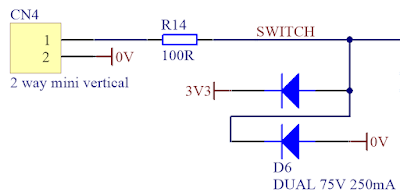
The flyback diode for the buzzer was omitted in the original design however one of the larger Schottky diodes was added as a footnote in the schematics. This diode was hand populated.

As the Schottky is expensive compared to a general-purpose diode, the dual diode was used.

Launcher Updated Buzzer Diode

High Side FET Reverse Protection
The protection components for the VN7040 consist of a diode and resistor. A 4.7 k resistor was used as part of the circuit.

As the 4.7 k resistor was the only part on the board, the resistor was changed to a 5.6 k.

Launcher Updated High Side Protection Resistor

FET to PSoC Interface Resistors
There were individual 10 k resistors which connected between the PSoC and the FET drivers.

The individual resistors were replaced with a new part, a single 10 k resistor pack.

Launcher FET Resistor Pack Update

PSoC Programming and Debug Resistors
The individual 100 R series resistors used between the external programming and debug connectors were replaced with a pair of 100 R resistor packs.

Launcher Debug Interface Resistor Pack Update

Launcher Programming Interface Resistor Pack Update

Part Changes
Part changes are usually instigated for several reasons. Some of these reasons may include using the same component type, to reduce the number of different part manufacturers, minimise components which are difficult to source or use parts already available in the current or similar designs.

Launcher Connector
An uncommon pluggable connector (3-pin Canon style) was used in the original design for connection to the launcher igniter. This connector was replaced with the identical 4-way 5.08 mm pluggable connector used for the battery input.

Launcher Igniter Connector Update

PCB Hardware
Buzzer Mounting
The buzzer was fitted as right-angle part to the PCB on the original design. In a Production environment during board assembly (loading), hand placement (manual) soldering of the buzzer would be required.

Buzzer Original Right Angle Mounting

To simplify board loading, the buzzer was changed from a right angle to standard thru-hole mount component on the bottom layer. As the buzzer is provided on a reel from the manufacturer, no hand population would be required.

Top Layer LED’s
The only surface mount components remaining on the top layer of the PCB were the Bluetooth and Status LED's. These LED's could be considered optional parts.

Launcher Original Status and Bluetooth LED's

The LED’s were changed to a bottom layer (rear) type which illuminates from the rear of the board. Although rear mount LED’s are usually more expensive, the cost to manually populate the two LED’s or reflow the board a second time to maybe a more expensive option.

Mounting Posts
To provide space between the Launcher board and the mounting plate inside the enclosure, M3 x 50 mm zinc-plated steel posts were used. The OLED was spaced with M2.5 x 15 mm zinc-plated steel posts.

The original M3 posts were removed and new M2.5 x 50 mm posts were selected. Technically not an improvement directly, however removing the M3 holes allowed a reduction in the PCB shape.

PCB Dimensions
The schematic changes detailed in this post were pushed to the PCB. As shown below, some rearrangement of routed component blocks was performed.

Launcher Schematic Updates Pushed to PCB

PCB Update
The schematic changes and updated component placement facilitated a reduction in board dimensions. Board dimensions were changed to 82 x 69 mm.

Launcher Updated PCB

Some signal traces were re-routed although the majority of existing signal traces were unchanged. Redundant tracks and micro planes were removed from the internal power planes of the PCB. These micro planes related to the UHF receiver.

Updated Launcher PCB 3D Bottom Side

Change Outcomes
The reduction in the PCB shape yielded a 29 % reduction in overall usage across the panel. This percentage is less if based on the actual bare PCB area.

Updating the schematic with the changes detailed in the blog resulted in a reduction to the number of components from 68 to 53 parts and the number of different types changed from 30 to 28.

Some new part lines in the form of resistor packs were introduced as a result of minimising components.

Final Thoughts
This blog provided a minimalistic review of the Launcher PCB with an indication of changes to suit manufacturing.

A further review for cost reduction to suit manufacturing may mean that the Cypress Bluetooth module would be integrated into the Launcher PCB. The switch-mode power supply could be changed to a linear supply to simplify the design. The pluggable connectors on the PCB could be removed and replaced with wires because the PCB is not unplugged regularly. Additional changes could be made to the Launcher design with each change likely to impact areas outside the cost and ability to manufacture the PCB in a production environment.