Showing posts with label salvage. Show all posts

Sunday, 30 April 2023

Salvaging from LG Controller Board EBR369328

Introduction
This microblog reviews the electronic components (parts) that could be salvaged from an LG air conditioner compressor inverter controller board.
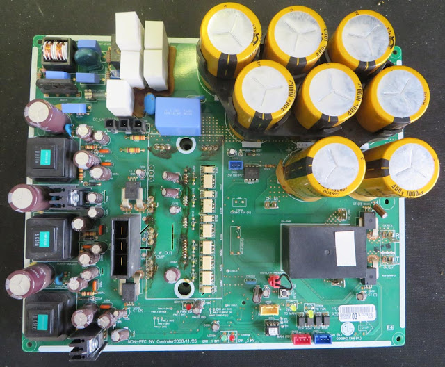

LG Control Board EBR369328 Top Side

Summary
After being provided with the inverter controller board for spare parts, it seems relevant to detail salvageable electronic components in this blog.

Being unfamiliar with air conditioning (AC) equipment, AliExpress was used to identify the function which is listed as an LG three-phase inverter compressor (motor) control board.

It should be noted that the LG control board was supplied not working. In these instances when salvaging electronic parts, additional
testing and diligence should be taken.

Salvageable Top Side Components
For the current measurement on the three-phase supply, an Allegro device capable of + 50 A, part number ACS756 was utilised. The Allegro part is listed as obsolete however this does not prevent is being used again for testing a
design concept. This is one of the devices that should be tested once removed because of its use in the circuit.
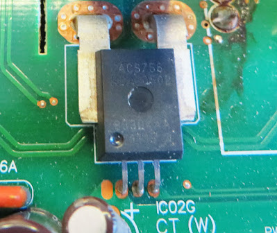
Allegro ACS756
Allegro ACS756

The bulk of the electrolytic capacitors are manufactured by the Korean company, Samyoung. Some of the electrolytic through-hole capacitors associated with the mains (line) supply may be handy for spares if mains voltage projects are an area of interest.
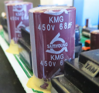
Mains Rated Electrolytic Capacitor

The large 10 to 20 W wire-wound ceramic resistors had no signs of overheating or physical damage. These resistors may be worth salvaging even for simple dummy loads.
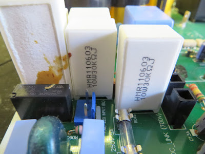
Wirewound Resistors
Wirewound Resistors

Located near the wire-wound resistors are mains capacitors manufactured by the Korean company, Pilkor. On this LG board, those capacitors were in excellent condition and worth salvaging.

Mains Capacitors
Mains Capacitors

The large vertical connector, AMP series D-5200, should be considered for anyone involved with high-current designs.

AMP Connector D-5200

The circuit board is fitted are a few different types of optocouplers. One of the interesting parts is the HCNR201 which is a high-linearity optocoupler from Broadcom.
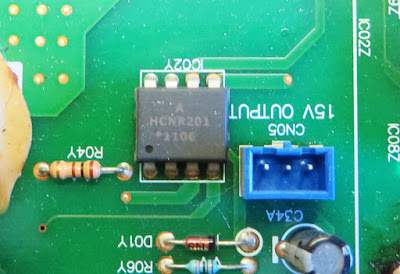
Broadcom HCNR201
Broadcom HCNR201

Other optocouplers include Toshiba TLP781, TLP559 and TLP521. All these Toshiba optocouplers are obsolete however they may serve well as spares or for repair purposes.

Various Toshiba Optocouplers

A TE relay with the part number T92S7D12-12 is fitted to the board. This relay is rated at a 12 V at 20 A and is still actively manufactured by TE.

High Current TE Relay

Contained on the board are a plethora of remaining components to consider for salvage. These include an oscillator, heatsinks, LEDs, chokes, axial resistors and unidentified components.

Salvageable Bottom Side Components
Fitted on the bottom side of the PCB is the motor switching module (IGBT). This device is most likely not worth salvaging.

Motor Driver Module
Motor Driver Module

The semiconductors on the bottom side appear to have no identification markings or those markings have become obscured by what appears to be a protective (conformal or lacquer) coating.
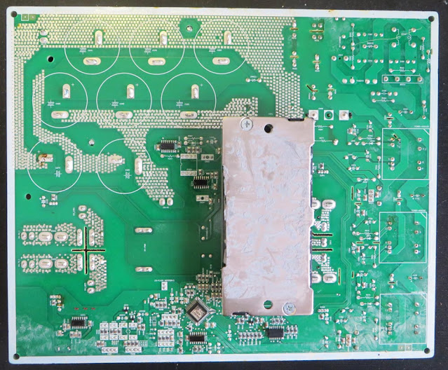
LG Control Board EBR369328 Bottom Side

All electronic parts on the bottom side of the board are epoxy glued to the as part of the circuit board assembly process. There is little to salvage from this side of the board because of the glue although removing components is possible with the correct tools. For low-cost and high-throughput printed circuit board assemblies, soldering using wave solder in a single pass has been a common manufacturing method. This LG board employs some solder-thieving designs in the circuit board layout as pictured below.
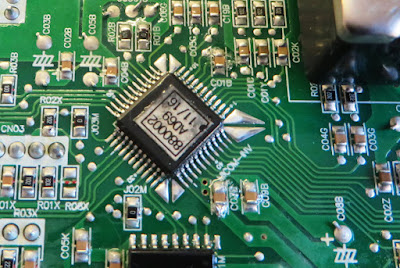
Component with Solder Thieving Pads

Monday, 26 September 2022

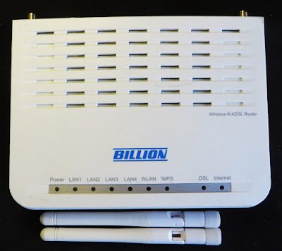
Salvaging Billion BiPAC 7700N

Introduction
This
blog illustrates portions of hardware that can be salvaged from a Billion ADSL model BiPAC 7700N R2.

Billion BiPAC 7700N R2 ADSL Modem
 
Salvaging
The Billion model 7700N contained two user-fitted external antennas and an AC wall adaptor DC 12 V 1A. Due to the age of the antennas, the plastic around the screw portion of the antenna was perishing. Reusing would be possible since the plastic on the connector does not affect functionality.

Billion ADSL Modem Antennas

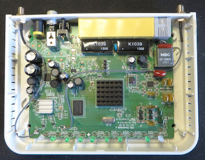
To access the internals of the modem, the four rubber feet on the bottom side of the model hide the plastic screws. Removing these allows access to the circuit board. For anyone with a 3D printer or repair cafe, the four plastic screws could be of use.

Billion BiPAC 7700N Internals

Two gold-plated SMA connectors can be salvaged however these are chassis mount and may not suit all designs.

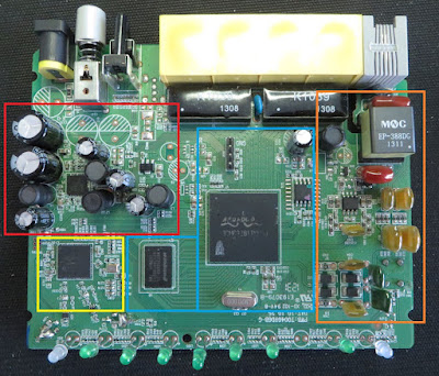
Billion BiPAC 7700N Circuit Board

The two small aluminium heatsinks were easily pried off the Broadcom chips. Either the smaller silver-coloured heatsink (11 mm x 11 mm) or the larger black-coloured heatsink (20 mm x 20 mm) could be repurposed on other designs or single-board computers such as the Raspberry Pi.

Billion BiPAC 7700N Circuit Board (ID Blocks)

The summary below relates to the components in the areas identified by the coloured boxes in the above image.

Red Box
The power supply uses a Texas Instruments triple output buck converter, TPS65251. The internal MOSFET resistances are suitable for a project; the overall efficiency is quite reasonable.

The passives surrounding the buck converter device are the support capacitors (EFC) and inductors. These parts could be salvaged if needed.

The associated right-angle PCB mount DC power jack and push-button power switch could be salvaged. It is presumed that the number of DC jack mating cycles and push-button switch actuations was minimal therefore repurposing would carry low risk.

Yellow Box
The Wi-Fi interfacing was managed by the Broadcom BCM43225 chip; likely not worth salvaging. Providing the clock for the Wi-Fi chip is an external 20 MHz crystal, worth removing as this is a standard 4-pin device.

Blue Boxes
The main CPU is a Broadcom BCM63281TK; likely not worth salvaging. Both the Macronix MX25L6445E serial flash and Winbond 256 Mb DDR2 DRAM W9725G6KB-25 may be useable devices. The external HC49S 20 MHZ crystal could be removed.

Orange Box
ADSL communications are handled by the Broadcom ADSL driver 6301KSG; only worth salvaging if required for repair or other projects. The associated ADSL line components, such as the line transformer and capacitors (100 V) would be worth salvaging for related projects or repairs.

Sundry Items
The remaining RJ-styled connectors and leaded LEDs could be salvaged for other projects.

Billion BiPAC 7700N Circuit Board Bottom Side

Flipping the circuit board over shows the reset switch and the obligatory passives such as inductors and decoupling capacitors. These passive components are not usually worth salvaging however as with any hardware salvage, the devices are based on the requirement.

Sunday, 31 October 2021

Salvaging Swann DVR SWDVR-81500H

Summary
This blog details the salvaging process of hardware from a Swann DVR, model SWDVR-81500H and an associated dome camera.

Swann DVR
Swann DVR
DVR
The Swann DVR unit was factory supplied with an external power supply and several dome cameras. This unit in this post was a superseded model.

Swann DVR Rear Plate

On the backplate of the DVR were inputs for the dome video cameras, audio inputs, video out, power, LAN and USB connections.

Swann DVR Internals
Swann DVR Internals

To open the DVR unit, four plastic screws in the base were removed. Upon sliding the metal plate away from the ABS case, the controller card and hard drive were visible.

The white ABS case was relatively sturdy and could be repurposed for another custom project. Similarly, the metal frame could be repurposed.

Hardware
The hard drive was held on with an additional four screws and easily removed. Manufactured by Western Digital, for this model DVR a
500 GB HDD was fitted. The drive could be reused; reformatting and standard SMART hard drive tests would be recommended.

Short Hard Drive Cables

The hard drives short serial ATA cable and power could be salvaged for another Single Board Computer (SBC) project.

To remove the controller board the screws in the metal base and backplate were removed.


Controller Card Components
Depending on the requirements of the salvager, most of the connectors from the controller board could be repurposed. The BNC connectors were sturdy and come with the right angle PCB mounting brackets. Most of the connectors were unbranded so cross-referencing against standard PCB footprints would be recommended for consistency and availability.

DVR Controller Board
 
Other parts such as the Piezo buzzer and CR1220 surface mount battery holder (yellow box in the above image) are readily salvaged.

Some of the electrolytic capacitors close to the DC input power jack were showing early signs failure with bulging at the top of the can.

The crystals, inductors, processor heatsink and LED's can readily be removed for salvage.

The controller was manufactured by HIKVision and the associated DDR3 memory (128M x 16) was from Samsung, part K4B2G1646F-BCK0 (blue box).

Processor Heatsink
Processor Heatsink

The controller was manufactured by HIKVision and the associated DDR3 memory (128M x 16) was from Samsung, part K4B2G1646F-BCK0 (blue box).

HIKVision Processor Cover

These parts were not worth removing unless required to repair another unit or similar DVR; the usual removal method would be via a hot air tool.

For the video decoding, an Intersil (Renesas) TW2968 8-channel video/audio decoder (orange box) was used by the DVR, likely not useable.

Ethernet communications utilised the Realtek 10/100 PHY, RTL8201F (purple box). Similar part here. The Ethernet chip supports the standard communications modes except RGMII. Could be salvaged using the correct tools however Gigabit devices are more common.

For timekeeping, an NXP RTC PCF8563 on the rear of the board was used. The RTC has a standard SOIC footprint which is worth salvaging with the battery holder (yellow box ) for a project requiring an RTC.

Lastly, the DC 12 V 2 A plug packs powering the DVR were in reasonable condition, with a larger style DC jack; worth keeping as spares.

Camera Hardware
The associated DVR dome camera presented as a sealed unit. The body of the camera was produced from diecast aluminium.

Dome Camera
Dome Camera

After removing the dome camera from the plastic roof mount, three screws were visible on the rear of the camera. Removing the screws on the rear allowed the cover containing the glass window to be taken off.

Dome Camera Opened
Dome Camera Opened

Looking at the internals of the camera, the LED ring is immediately visible. Removing the two retaining screws and the connecting cable allowed the LED ring to be removed.

Dome Camera LED Ring

The twenty-four IR LED’s fitted to the PCB could be salvaged. However, the board is a self-contained circuit, with a light sensor and LED driver which may suit a project requiring IR illumination without modifications.

Dome Camera LED Ring Rear

Holding the camera board to the diecast aluminium base were M2.5 bolts and M2.5 x 13.5 mm Hex metal spacers. The two halves of the dome camera could be repurposed for another camera project.

Dome Camera Board
Dome Camera Board

The camera board contained a day-night switch which was achieved using a mechanical assembly.


Camera Day-Night and Lens Assembly

This assembly also contained the camera lens. Driving the day-night switch solenoid was a Unisonic reversible motor driver BA6208.

Camera Board Front
Camera Board Front

Removing the camera chip would be possible, however desoldering all four sides of the device usually requires dedicated equipment or patience.

Camera Board Rear
Camera Board Rear

Interfacing to the camera chip and controlling the solenoid for day-night operation was an ST microcontroller, part STM8S003F3P6. With 8k of FLASH memory and a small amount of EEPROM, this could also be salvaged.

The switch-mode power supply manufacturer was not identifiable.

The remaining parts such as the 27 MHz crystal, inductor and surface mount connectors (reasonable quality) could also be salvaged.

Other items such as the BNC adaptors and interconnecting cables between the DVR and dome cameras were not worth salvaging.


Thursday, 22 November 2018

Salvaging electronic parts - Part 3 BenQ GL2430 Monitor

Summary
This blog continues a series of salvaging electronic parts, this time focusing on a BenQ model GL2430 monitor and what components could be salvaged. 


GL2430-B  BenQ Monitor
GL2430-B  BenQ Monitor
The monitor build date was from early 2011.


GL2430 Name Plate
GL2430 Name Plate

Salvaging
The dismantling process for the monitor was skipped. The two major and two smaller printed circuit boards (PCB) removed from the monitor were: Flat panel driver board, Power supply board, Backlight driver board and Audio breakout board.

Flat panel driver board
Shown below is the flat panel driver board, single sided multilayer circuit board. This board contains the Realtek flat panel driver IC boxed in blue. Realtek part RTD2483RD. 


GL2430 Flat Panel Driver Board Top Side
Boxed in red of the image are a mixture of five serial memory devices ranging from ST Micro 24C02 EEPROM to a Winbond 2Mbit Flash W25X20. These devices are usually very easy to salvage.

Boxed in yellow are some of the numerous inductors on the board.

The semiconductor in the top right hand corner of the image is a Diodes Inc PAM8603 - 3W stereo class D amplifier. Possibly not worth salvaging as there are parts available with lower distortion ratings.

In the bottom left hand corner of the board are a pair of TVS arrays from the manufacturer InPaq 1045QU. Again probably not worth salvaging.

The crystal on the board is common video 14.318MHz type and could be repurposed if any crystal frequency is suitable.

Remaining on the board are a mixture of connectors, passives and unidentified semiconductors. If you were really scratching to find a MELF diode or 220uF Lelon Electrolytic then this board could be added to the spare parts box.

Power supply driver board
The power supply board is populated with components on both sides, double sided with a single layer PCB design. Heavy through hole components on the top side of the PCB and smattering of glued surface mount components on the solder side.


GL2430 Power Supply Board Top Side
Boxed in red is the mains common mode choke and towards the centre of the board, the switching transformer. Both these devices are manufactured by a Taiwanese transformer manufacturer. These parts can come in handy for research and design projects and a worth salvaging.

The green boxes highlight a few resistors which could be extracted for the spares bin. There are no signs of overheating or other physical damage which may have been caused by a fault on the PCB.

In the blue boxes are the diodes and bridge rectifiers. The bridge rectifier is listed as an obsolete part on supplier's websites such as Mouser so may be good for the spare parts box. The two larger axial diodes are Vishay part UG4B; a reputable brand worth salvaging once properly tested.

The two devices on heatsinks are the mains side switching MOSFET K4101 and secondary side dual rectifier diode FMX12S. At least one of these devices has discolouration in the PCB surrounding the heatsink. Heatsinks could be salvaged for other purposes.

Remaining on the top side of the board are various connectors, mains voltage rated varistors and mixture of capacitors. Usually components which have been operating at mains voltages for an unknown amount of time can left on the PCB if the operational state of these parts is unknown.


GL2430 Power Supply Board Bottom Side
Shown above is the solder side of the power supply board. To the left of the image is the switch mode controller. Across the board are a number of other parts, all glued down with epoxy. Using epoxy to glue surface mount components in order to simplify the assembly process is standard practice. The epoxy can make repair and salvaging parts difficult.

Backlight driver board
Below is an image of the backlight driver board. The main LED driver, boxed in red, is an MP3389 from Monolithic Power. Device is worth salvaging or even the entire board itself as it is a self-contained unit which could easily be reused.


GL2430 Backlight Board Top Side
Boxed in blue is an unbranded inductor which is always good to have in the spares box.

Shown in the yellow box is a SinoPower MOSFET APM1110 which was not located on the company website. Specifications are nothing to be excited over although part would be worth salvaging for prototyping.

The remaining passives such as the radial capacitors are from Lelon making the remainder of the board a contender for the spares box.

Audio Connector board
Lastly is the small 3.5mm audio connector board. The connectors are a standard pinout and could be salvaged or the entire board repurposed for a bespoke project.


GL2430 Audio Connector Board Top Side

Design Notes
A section of the power supply mains input section was chosen for some brief notes on PCB design.


GL2430 Power Supply Board Main Input Section
Boxed in white, top left hand corner of the above image, is the one of the mounting holes with exposed long pads coated in solder. This is a good feature for eliminating star or copper washers however the electrical resistivity can suffer due to the smaller contact area and surface oxidisation of the solder. It should be noted that on the component side of the board is a through hole nut allowing direct access to the mains earth connection.

In the orange boxes are several slots on the board to improve the creep distance between component pins. Slots in the board are an effective and cheaper solution to conformal coating.

Shown in the blue box is attention to detail by the PCB designer. A small pullback was applied to the copper surrounding the two mounting holes for the IEC mains connector.

Boxed in purple is a section of silk screen showing the isolation plane between mains AC and isolated DC voltages. The silk screen for the isolation plane and most components is present on both sides of the PCB making component identification and servicing easier.

Lastly the red box shows three cascaded surface mount resistors used in series to discharge the mains input capacitor connected between active and neutral. The PCB designer was mindful of creep distance and to some degree spacing between these components.

Tuesday, 3 July 2018

Salvaging electronic parts - Part 2 Spark Gaps

Summary
This blog is a continuation of a prior blog which illustrated the selection of electronic parts for salvage and basic component removal using a soldering iron.

Salvaging Designs
As used in the first part of the Salvaging Electronic blog, the same NESS security system (D8X D16X) control board will be used for the purposes of this blog. The content of this blog focuses more on salvaging, replicating or repurposing designs. When referring to designs this could be the schematic design, Printed Circuit Board (PCB) layout or both.

The section of Ness control PCB under examination in this blog was the sensor input. This area was chosen was to illustrate the schematic (resistors selection) and PCB design (on-board spark gaps).


Ness Sensor Input Section
The image above shows the passive components related to monitoring devices such as relay contacts (PIR sensors). 

A basic schematic representation of one of the input channels is shown below. Note that this hardware design operates in an analogue fashion. That is, the voltage on each sensor input is fed into an analogue switch (4051) and measured by the on-board controller. A break in the line between the externally connected sensor and the sensor input circuit changes the voltage measured.

Of interest in this design is the line facing input resistor (Rb) and the spark gaps (Ya).

Sensor Input Section
How is this design useful? 

When designing a product, with similar specifications, then referencing existing and proven designs can serve as a valuable baseline. This is not to say that newer solutions or devices should not be investigated thoroughly. Consider a product with a similar input requirements such as an external automated gate, marine access hatch monitor or cattle feed flow controller which may require external monitoring of a sensor. A similar input circuit would seem a logical choice. Could the input resistor Rb be exchanged with a standard thick film resistor (1206 footprint)?

Looking at a standard Panasonic 1206 resistor, this part is rated at a continuous 200V for a maximum power of 250mW. For steady state conditions this voltage and power handling would be more than suitable. In some systems, inputs can be subject to transient voltages as a result of external events which may be due to indirect lightning strikes for example. Using a single standard thick film resistor may not be the ideal choice for this solution. 

Undoubtedly for transient events, additional protection such as Varistors, Transorbs or other surge protection solutions are commonly used in conjunction with suitably rated circuit components. Inputs circuits are usually bolstered using devices designed for handling transients (Pulse Withstanding) such as Metal ELectrode Face (MELF) resistors. MELF devices from Vishay are such an example. The Vishay series MMA HV MELF in an 0204 footprint (1206 compatible), operates at a continuous 300V for a maximum power of 400mW
For the same footprint and small increase in cost, an input section can be made more robust. This provides the option of switching between standard vanilla and application specific components.

Salvaging Layouts
For the sensor input section, it was mentioned earlier that for transient events other surge protection solutions could be added to the design.


Ness Sensor Input Spark Gap
The Ness board has two solutions for line facing transients. One is circuit components (Yb and Yc) and the second is exposed PCB traces (Ya). Components Yb and Yc are most likely Varistors and Ya is an array of several spark gaps made possible by sections of PCB copper with solder mask removed. It should be noted that component Yb is not fitted to the board in lieu of Ya being 'on the fibreglass'. Certainly Varistors are more accurate for a rated breakdown voltage when compared to a spark gap and add cost to the board. 
A spark gap, as the name suggests, is a gap or distance between two points across which a transient voltage (spark) can discharge. The distance the spark can breach is a function of creep distance. Technical literature on this subject can be viewed at multiple sites such as EDN Access (basic) - ESD Protection for IO Ports, read on Stack Exchange, Wiley, PTR or the distance needed for a design can be calculated on www.creepage.com. Some understanding of material and contamination of PCB's is required.

For those needing a fundamental understanding of creepage, Paschen's law is a solid starting point.

Focusing on the Ness control PCB, the gap between the two spikes is somewhere around 1mm. Using the tables on the PTR website to determine a ballpark transient overvoltage, for a standard level two PCB contamination on FR4 PCB, yields approximately 400V.

In reality 400V is an extremely low voltage for arcing and only marginally above the theoretical 327V required to arc in one atmosphere of air, see Paschen's law. Regardless of the actual breakdown voltage of this design, some level of protection will be afforded to the design with the addition of spark gaps to the PCB. In any event component, Yc will bear the brunt of any residual voltage that the spark gap does not dissipate.

Adding Spark Gaps to a PCB
Depending on your drafting software of choice, the process to add spark gaps may differ from program to program. The subsequent method described requires only changes to the PCB file however, is not the only method for implementing spark gaps in a PCB design. Some designers may prefer to create the spark gap as a schematic / PCB component library pair or modify existing library components to facilitate the additions of spark gaps. Each method has its own merits and should be reviewed carefully.

The target design for adding spark gaps was the Solar MPPT Project designed in a previous blog. There are two external digital lines which provide communications between an MPPT and a Solar MPPT Controller. These TTL lines expose both the MPPT and Controller to transients and use only steering diodes for protection.


Existing Communications Port - No spark gap
A spark gap separation of 0.5mm was used for the purposes of illustration. For a specific design, the necessary calculations should be made to determine the correct separation.

Fortunately there are ample 0V connections on the existing communication connector. Other designs may need to make use of vias to provide the necessary return path for the transient event.


Top Layer Spark Gap Added
In the above image, a polygon was added to the solder side of the component - top layer. A single pair of terminals 'points' for the spark gap is sufficient if the chance of the design experiencing a transient event is low. For higher probability of transient events, then more points should be used where practical for the design.
Top Side Solder Mask Over Spark Gap
Following the addition of the copper to the board the solder mask must be excluded from the region used by the spark gaps. The capture above shows the spark gaps with the solder mask included.


Fill Added - Top Layer Solder Mask
Fill Added - Top Layer Solder Mask 
To exclude the solder mask, a fill was added to cover the area over and between the spark gap terminals.


Top Side Solder Mask Removed Over Spark Gap
Viewing the addition of the solder mask fill to the board shows the exclusion over the spark gap terminals. In some instances the PCB terminals are given a liberal coating of solder at the time of assembly. The main goal is to lengthen the lifespan of the terminals.

Whether components, an input design or PCB layout is recovered from the occasional tear down or salvage, the process can be well worth the exercise.