Friday, 19 June 2020

Salvaging Parts BiPAC 7800VDOX

Summary
This post details which circuit board components could be salvaged from a Billion BiPAC 7800VDOX Wireless Router.

BiPAC 7800VDOX Wireless Router

Router Disassembly
To separate the Wireless Router's grey lid from its base, four rubber feet located on the base of the router enclosure were removed. The removed feet expose the screws retaining the lid.

BiPAC 7800VDOX Wireless Router PCB

The above image shows the Wireless Router internal Printed Circuit Board (PCB) with the light pipe and rear panel removed.

Parts to Salvage
Cabling
There are two antennas in the lid with RF connectors (RSP / AMC style) which could be salvaged.

Heat Spreaders
On the PCB are several ceramic heat spreaders (heatsinks) attached to various Broadcom components. These are held down with double-sided tape.

Mounted Heat Spreaders

Removing the heat spreaders can be achieved using a tool such as a wide flat blade screwdriver to lever the heat spreaders off carefully.

7800VDOX Wireless Router PCB No Heat Spreaders
7800VDOX Wireless Router PCB with No Heat Spreaders

Removing the heat spreaders exposes the Broadcom chipsets comprising of the processor, RF and communication hardware. The Broadcom hardware is not suitable for salvage, possibly repair to a similar router.

Inductors
There are open core leaded and PCB mount inductors which could be recycled for other designs.

Wireless Router PCB Inductors

Diodes
Identified in the image below are single and dual colour surface-mount LEDs.

Wireless Router PCB LEDs

Oscillators
A 25 MHz thru-hole Crystal is located next to the Broadcom chip responsible for the Ethernet clock and a second surface mount Crystal oscillator can be found by the Broadcom processor.

Wireless Router PCB Oscillators

Relays
The two Fujitsu FTR-C1CA003G miniature relays have a coil operating voltage of 3 V DC with DPDT 1A contacts. These thru-hole relays are worth removing.

Wireless Router PCB Relays
 
Resistors
Distributed across the top and bottom side of the PCB are resistors with case sizes larger than 0805 which can be repurposed. Most are standard resistor values.

Wireless Router PCB Resistors

DC-DC Regulators
A mixture of Fitipower DC-DC Step Down Switch mode chips (FR98860 and FR9888) could be removed.

Wireless Router PCB DC-DC Controllers

Connectors
The vertical USB connector and DC jack could be removed and reused in another design. Removing and reusing the right-angle Ethernet or RJ connectors should be achievable.

Capacitors
Any of the radial Electrolytic capacitors could be reused. It should be noted that the Su'scon capacitors (SD and SK series) although rated with a useful operating temperature of 105°C (max), have a 2000 hour operating life at the maximum rated temperature. Consider that the Wireless Router may have been operating for 10 years continuously which may have significantly reduced the lifetime of the capacitor.

The other surface-mount Electrolytic capacitors (22uF) appear to be the Panasonic FK series which are rated to 105°C with a 2000 hour operating life at the maximum rated temperature.

Wireless Router PCB Capacitors

Unlisted Components
Several additional types of components could be removed from the Wireless Router PCB although some are extremely small (0402 footprints), obsolete or specific to the product. The components listed in this post should have equivalents from different component manufacturers allowing salvaged parts to be used in a prototype PCB design or used for repair.

Monday, 1 June 2020

Mikroe Buck 5 Click with PSoC5 VDAC

Summary
This post examines alternate means for driving the MikroElektronica Buck 5 Click hardware. First, the onboard digital Potentiometer was rewired in a new configuration and second the Potentiometer was replaced with Cypress PSoC.

Buck 5 Click - Courtesy MikroElektronica

Buck 5 Click with Digital Potentiometer and PSoC5
MikroElektronica's Buck 5 Click (MIKROE-3100) hardware presented itself as a cost-effective and off the shelf unit for testing the MAX17506 DC-DC Converter. The Buck 5 Click was designed primarily for use with other MikroElektronica hardware. The input voltage range of the Maxim buck converter (4.5V to 60 V DC) is not fully utilised on the Buck 5 Click (5V to 30 V DC). In the same manner, the output voltage appears capped at 20 V DC maximum. Even with the voltage limits the output range of the hardware was able to be tweaked. 


Wiring a Cypress CY8CKIT-059 prototyping kit to drive the Buck 5 Click required three connections for the SPI and two for power. The Buck 5 Click schematics indicated the board logic operated with 3.3 V DC however, the board was powered from 5 V DC. The supply range of the MAX5401 digital Potentiometer (pot) was 2.7 V to 5.5 V DC.

To control the digital pot, a PSoC Creator application using an SPI Master component was created


SPIM_WriteTxData(Buck5_Dig_Pot_Val);
while (0u == (SPIM_ReadTxStatus() & SPIM_STS_SPI_DONE)) 
{ }


The subsequent step of increasing the output voltage range of the Buck 5 Click was accomplished although the configuration of feedback resistor network (R8) and digital pot (U2) for the DC-DC converter (MAX17506) needed to switch places. The digital pot operating voltage was the reason for the change. The pot wiper was connected directly into the feedback pin of the MAX17506. Below is a working board with modifications.


Buck 5 Click Modified with Increased Output Range


The output voltage range of the modified board was approximately 4V to 18 V DC. The digital pot, with 255 positions, provided output voltage steps of 55 mV.

When applying power to the digital pot, the default setting is the middle position which may not be ideal in all instances. To control the behaviour of the buck regulator on power-up, a connection from the PSoC to the Enable line of the Buck 5 Click was used. A pull-up resistor (R4) was removed from the board to prevent the Buck 5 Click from starting when power was applied

Buck 5 Click with Cypress PSOC5 VADC, No Digital Potentiometer
Other solutions for adjusting the output voltage of a DC-DC converter, through control of the feedback pin, use external PWM or DAC sources.

The Cypress PSoC provides control of DC-DC converters either through PWM (Trim and Margin component) or a DAC (Current or Voltage component). This post used the PSoC VDAC8 component which provided 255 steps. For additional resolution the dithered VDAC component with 4096 steps could be used.

For calculating the output voltage for VDAC solution, Maxim published a notable tutorial deriving the output equation shown below from first principles.

VOUT = VREF(1 + (R1/R2)) + (VREF - VDAC) (R1/R3)                        Eq (1)

For connection of the VDAC to the feedback loop of the DC-DC Converter, one additional resistor (R3) was required.


DC-DC Converter Output Voltage Control Using a DAC

A spreadsheet was used to implement Equation (1) which allowed the three unknown resistor values to be manually changed and the output voltage range of the DC-DC converter observed.

DC-DC Converter Vout Spreadsheet Calculations

Equation (2) was used to ensure that the maximum current seen by the PSoC (DAC) was less than 25 mA.

i3 = (VREF - VDAC)/R3                       Eq. (2)

Quadrature Encoder
A quadrature encoder (Bourns PEC11R) was added to the design to allow for manual voltage adjustments. The QuadDec component was used to convert the encoder AB lines. The QuadDec returned value was limited to between 0 and 255. The reading from the QuadDec was then used to adjust the output of the VDAC component.


PSoC Creator Top Design
The project required the QuadDec, DAC and OpAmp components as shown below.


PSoC Creator Project Top Design


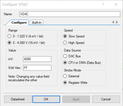
The calculations in Excel used a voltage range from 0.1 V to 4.08 V which was the option selected in the VDAC component.

VDAC Component Settings

While not essential, an OpAmp follower was added to the design.

OpAmp Component Settings

To maintain 255 positions the QuadDec component was changed from the default 8 bit to 16 bits.

QuadDec Component Settings

The remaining signals that are shown on the PSoC Creator project page (Top Design) were related to the DC-DC converter (PSU_Enable) and the on-board switch (Switch1). Voltage ramps were generated in code on start-up then Switch1 was pressed.

To facilitate testing of the encoder, a UART component was added to the project.

PSoC Creator Pin Mapping
Pin mapping for the design is shown below.


PSoC Project Pin Mapping


PSoC Creator Code
Listed below is an extract of some quick and grubby code used for testing the Mikroe with the PSoC Creator prototyping board.


/**
* @brief Main init and update VDAC based on quadrature encoder value
*/
int main()
{
  uint16_6 Encoder_Count, Encoder_Count_last = 0;
CyGlobalIntEnable();
QuadDec_Start();
UART_Start();
Opamp_Start();
VDAC_Start();
CyDelay(2000); /* Time to stabalise */
PSU_Enable_Write(true); /* Switch DC DC On */
pulse_on_switch1();
for(;;)
{
Encoder_Count = QuadDec_GetCounter();
if (Encoder_Count != Encoder_Count_Last)
{
if ((Encoder_Count <= MAX_ENC) && (Encoder_Count >= MIN_ENC))
{
write_to_uart(Encoder_Count);
VDAC_SetValue(Encoder_Count);
}
else if (Encoder_Count > MAX_ENC)
{
Encoder_Count = MAX_ENC;
QuadDec_SetCounter(MAX_ENC);
}
else if (Encoder_Count < MIN_ENC)
{
Encoder_Count = MIN_ENC;
QuadDec_SetCounter(MIN_ENC);
}
Encoder_Count_Last = Encoder_Count;
}
}
}

The functionality of the test code was to read the Quadrature Decoder, ensures the value read was within the range, then write the value to the VDAC.


Hardware Setup
Shown in the image below is the hardware setup which consisted of the Buck 5 Click, PSoC board and the rotary encoder.


Buck 5 Click with Increased Output and PSoC VDAC

Output Voltage Range and Regulation
The calculated output voltage range was for 1.62 V to 20.33 V DC and the measured range was 2.39 V to 20.42 V DC.

Rudimentary load tests were conducted with a resistive load driven by the Buck 5 Click. Tests indicated a 0.25 % voltage regulation with low loads (1W) and better than 0.1 % with higher loads (65 W). The DC-DC converter used in the Buck 5 Click (MAX17506) has a capability of 5 A. The full load current was not load tested.

Output Voltage Adjustment using PSoC
To change the output voltage of the DC-DC converter without the encoder, the value written to the VDAC was controlled in software. When the switch located on the Cypress CY8CKIT-059 prototyping kit was pressed on power-up, the code generated several pulse types.

Buck 5 Click Output Voltage Waveform from PSoC VDAC
Buck 5 Click Output Voltage Waveform driven from PSoC VDAC

The capture above shows the Buck 5 Click output voltage ramp up and down with a 220 R resistive load.

Final Thoughts
The MikroElektronica Buck 5 Click was a reliable hardware module which allowed a Cypress PSoC to be interfaced for testing. Using a DAC to adjust the output voltage provided an alternative method to the on-board Potentiometer. The option to use PWM control for voltage adjustment was not reviewed in this post although this method should be considered as another solution.


Downloads
PSoC Creator 4.3 Power Supply Project (PSU) Project.

PSoC Creator 4.3 PSU Project