Showing posts with label switch. Show all posts

Saturday, 31 August 2024

Making Amazon 9.8" Pottery Wheel Foot Switch Detachable

Introduction 
In this blog, a modification was made to the generic 9.8” pottery wheel supplied by Amazon. A connector was fitted to allow the foot pedal to be removed.

Amazon Pottery Wheel (Courtesy Amazon)

Pottery Wheel Foot Switch Cable Location
Protruding from the underside of the pottery wheel is a white cable that connects the foot pedal to the pottery wheel’s electronic controls. The connection of the white cable was altered to fit a connector allowing disconnection for movement or storage of the pottery wheel.

Underside View of 9.8" Pottery Wheel

The white cable passes through a hole in the pottery wheel's metal chassis. The hole's internal diameter is approximately 14.8 mm. Depending on the type of chassis mount connector selected, the hole may already be suitable for that connector. Alternatively, an inline pluggable connector could be fitted instead of the chassis mount connector.

An M12 chassis mount and an inline connector set from TE Connectivity was chosen for this project.

Pluggable Connectors
Fitting the M12 chassis mount socket connector started with cutting the white cable. Sufficient cable length was left protruding through the hole to allow for connecting to the chassis mount connector. The cable was moved to the side temporarily while the hole was made larger with a stepped drill bit.

The three wires in the foot pedal cable, red, yellow and green were stripped and tinned. A small length of heatshrink was fitted on each wire. The cable was passed through the retaining nut and then the hole in the chassis. The wires protruding through the hole were soldered to the M12 socket.

Pottery Wheel Side - M12 Chassis Mount Socket

For the mating side of the connector, an M12 plug was fitted to the cable attached to the foot pedal.

Foot Switch Side - M12 Inline Plug

The M12 TE Plug used screw terminals instead of solderable pins. The stripped wires were connected in the same order as the socket.

An operational test was performed before finalising the heatshrink and tightening the M12 nut.

Pottery Wheel M12 Connector Test Fit

The assembled foot switch is pictured below.
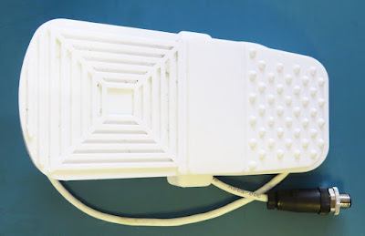
Updated Foot Switch Assembly

The connected assembly of M12 connectors is shown below.

Completed M12 Connector Assembly


Saturday, 24 February 2024

CTEK MXS 5.0 Pushbutton Switch Replacement

Introduction
This blog follows the process of replacing a faulty mode switch on a CTEK MXS 5.0 battery charger. The symptom of failure was no change in the mode when the mode button was pressed.

CTEK MXS 5.0 Charger
 
Repair Process

With no screws located on the charger case for servicing, YouTube was consulted on methods to open the charger.

For this charger model, the case is a two-part build. The sealing mechanism between the two cases (seam) appeared to be a glue or a plastic weld. The plastic seam was cracked by placing a flat blade (wide) screwdriver on the seam and striking the rear of the screwdriver with a mallet. The break in the plastic was, however, not entirely clean.

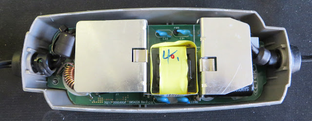
CTEK MXS 5.0 Open Case

On separating the case halves, the plastic base of the charger contains what appeared to be some type of isolator.

CTEK MXS 5.0 Case Bottom

CTEK MXS 5.0 Case Lid

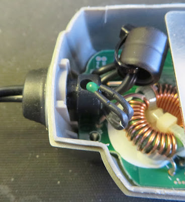
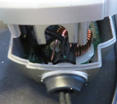
To allow access to the charger circuit board, the cable glands at either end had to be removed. As pictured in the image below, one of the glands has an indent for a thermistor or possibly a thermal fuse.

MXS 5.0 Device in Cable Gland

With the board unseated and flipped over, the logic devices, controllers, processor and switch were visible.

CTEK MXS 5.0 Circuit Board

Possibly to prevent damage to the decal, the membrane switch has a plastic cap fitted.

CTEK MXS 5.0 Circuit Board Switch Cap Off

As the pushbutton switch manufacturer and model were unknown, a similar surface mount switch was used. 

For readers preferring to locate an exact pushbutton replacement, the switch body is 6 x 6 mm with a height of 4 mm. The switch plunger height from the switch body is approximately 2.7 mm. The top of the tapered shaft is 3.45 mm. The top of the switch shaft is the side pressed into the button cap.

CTEK MXS 5.0 Factory and Replacement Switch

The plunger height of the replacement switch was manually reduced with a pair of side cutters.

After fitting the replacement switch to the circuit board, the charger was powered and the button operation was tested. The switch cap was then fitted.

CTEK MXS 5.0 with New Switch

Reassembly
The circuit board was moved into position and realigned to fit into the charger's plastic lid.

During the reassembly process, the electronic protection device was reinserted into the cable gland.

CTEK MXS 5.0 Protrusions for Cable Gland

When the two halves of the charger case were pushed together, the two U-shaped plastic protrusions on the plastic base locked the cable glands in position.

Lastly, to permanently join the halves of the charger case, glue was applied to the seams near the cable glands. For readers using the charger in a high moisture or damp environment, fully sealing the seam of the charger is highly recommended.

CTEK MXS 5.0 Charging Battery


Thursday, 26 January 2023

HPM D817SLIM Repair

Introduction
This short blog details the repair of an HPM main-powered digital switch timer, model D817SLIM. The fault symptoms are a blank LCD which does not restore even after the timer is plugged back into the mains.

HPM D817SLIM Mains Digital Switch Timer

Opening the Digital Timer
Disclaimer: Repair of any mains-rated electrical equipment should be conducted by qualified personnel. The information provided in this blog is for reference purposes.

The mains-powered timer (unit) had not been powered for several years and the LCD that displays the time and timer functionality was blank. Connecting the unit to the mains did not restore the operation of the LCD.

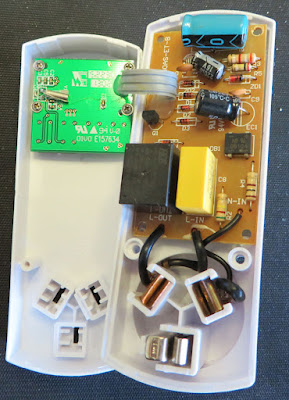
To open the unit, there are two plastic screws on the rear of the unit. The screws appear to be a Y-wing or a variant of that screw. A 2.4 mm wide flat blade was found fit the head pattern and the screws were removed. The two-piece plastic case uses internal clips so the same screwdriver can be used to unclip the case halves. There are circuit boards on either side of the plastic cases.

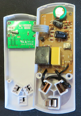
Internals of HPM D817SLIM Mains Digital Switch Timer

Dead Battery

Upon opening the case, a small Ni-MH battery with corrosion or leakage was visible on the circuit board. The part was identified as a Troily 1.2 V 80 mAh Ni-MH battery.

Troily 1.2 V Ni-MH Battery

Instead of replacing the battery, it was decided to use a standard electrolytic capacitor. If this unit was to be used in an area with frequent and long interruption to mains power, a battery replacement would be advised instead of the capacitor.

To remove the circuit board with the battery, two small Philips screws were removed.

Removed Troily Battery
Removed Troily Battery from HPM Circuit Board


Battery Replacement
The battery was then unsoldered and replaced with a 1000 uF 25 V electrolytic capacitor. Since the operating voltage of the mains timer circuit is less than 5 V, a 6.3 V capacitor with a larger capacity could likely be used. Testing showed that with a 1000 uF electrolytic capacitor, the switch timer remained powered for approximately 6 minutes after a mains failure.

HPM D817SLIM Mains Digital Switch Timer with Capacitor

Other options to repair the unit, such as replacing the Ni-MH battery with a similar type or using a supercapacitor may be possible.

Monday, 1 June 2020

Mikroe Buck 5 Click with PSoC5 VDAC

Summary
This post examines alternate means for driving the MikroElektronica Buck 5 Click hardware. First, the onboard digital Potentiometer was rewired in a new configuration and second the Potentiometer was replaced with Cypress PSoC.

Buck 5 Click - Courtesy MikroElektronica

Buck 5 Click with Digital Potentiometer and PSoC5
MikroElektronica's Buck 5 Click (MIKROE-3100) hardware presented itself as a cost-effective and off the shelf unit for testing the MAX17506 DC-DC Converter. The Buck 5 Click was designed primarily for use with other MikroElektronica hardware. The input voltage range of the Maxim buck converter (4.5V to 60 V DC) is not fully utilised on the Buck 5 Click (5V to 30 V DC). In the same manner, the output voltage appears capped at 20 V DC maximum. Even with the voltage limits the output range of the hardware was able to be tweaked. 


Wiring a Cypress CY8CKIT-059 prototyping kit to drive the Buck 5 Click required three connections for the SPI and two for power. The Buck 5 Click schematics indicated the board logic operated with 3.3 V DC however, the board was powered from 5 V DC. The supply range of the MAX5401 digital Potentiometer (pot) was 2.7 V to 5.5 V DC.

To control the digital pot, a PSoC Creator application using an SPI Master component was created


SPIM_WriteTxData(Buck5_Dig_Pot_Val);
while (0u == (SPIM_ReadTxStatus() & SPIM_STS_SPI_DONE)) 
{ }


The subsequent step of increasing the output voltage range of the Buck 5 Click was accomplished although the configuration of feedback resistor network (R8) and digital pot (U2) for the DC-DC converter (MAX17506) needed to switch places. The digital pot operating voltage was the reason for the change. The pot wiper was connected directly into the feedback pin of the MAX17506. Below is a working board with modifications.


Buck 5 Click Modified with Increased Output Range


The output voltage range of the modified board was approximately 4V to 18 V DC. The digital pot, with 255 positions, provided output voltage steps of 55 mV.

When applying power to the digital pot, the default setting is the middle position which may not be ideal in all instances. To control the behaviour of the buck regulator on power-up, a connection from the PSoC to the Enable line of the Buck 5 Click was used. A pull-up resistor (R4) was removed from the board to prevent the Buck 5 Click from starting when power was applied

Buck 5 Click with Cypress PSOC5 VADC, No Digital Potentiometer
Other solutions for adjusting the output voltage of a DC-DC converter, through control of the feedback pin, use external PWM or DAC sources.

The Cypress PSoC provides control of DC-DC converters either through PWM (Trim and Margin component) or a DAC (Current or Voltage component). This post used the PSoC VDAC8 component which provided 255 steps. For additional resolution the dithered VDAC component with 4096 steps could be used.

For calculating the output voltage for VDAC solution, Maxim published a notable tutorial deriving the output equation shown below from first principles.

VOUT = VREF(1 + (R1/R2)) + (VREF - VDAC) (R1/R3)                        Eq (1)

For connection of the VDAC to the feedback loop of the DC-DC Converter, one additional resistor (R3) was required.


DC-DC Converter Output Voltage Control Using a DAC

A spreadsheet was used to implement Equation (1) which allowed the three unknown resistor values to be manually changed and the output voltage range of the DC-DC converter observed.

DC-DC Converter Vout Spreadsheet Calculations

Equation (2) was used to ensure that the maximum current seen by the PSoC (DAC) was less than 25 mA.

i3 = (VREF - VDAC)/R3                       Eq. (2)

Quadrature Encoder
A quadrature encoder (Bourns PEC11R) was added to the design to allow for manual voltage adjustments. The QuadDec component was used to convert the encoder AB lines. The QuadDec returned value was limited to between 0 and 255. The reading from the QuadDec was then used to adjust the output of the VDAC component.


PSoC Creator Top Design
The project required the QuadDec, DAC and OpAmp components as shown below.


PSoC Creator Project Top Design


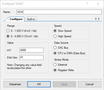
The calculations in Excel used a voltage range from 0.1 V to 4.08 V which was the option selected in the VDAC component.

VDAC Component Settings

While not essential, an OpAmp follower was added to the design.

OpAmp Component Settings

To maintain 255 positions the QuadDec component was changed from the default 8 bit to 16 bits.

QuadDec Component Settings

The remaining signals that are shown on the PSoC Creator project page (Top Design) were related to the DC-DC converter (PSU_Enable) and the on-board switch (Switch1). Voltage ramps were generated in code on start-up then Switch1 was pressed.

To facilitate testing of the encoder, a UART component was added to the project.

PSoC Creator Pin Mapping
Pin mapping for the design is shown below.


PSoC Project Pin Mapping


PSoC Creator Code
Listed below is an extract of some quick and grubby code used for testing the Mikroe with the PSoC Creator prototyping board.


/**
* @brief Main init and update VDAC based on quadrature encoder value
*/
int main()
{
  uint16_6 Encoder_Count, Encoder_Count_last = 0;
CyGlobalIntEnable();
QuadDec_Start();
UART_Start();
Opamp_Start();
VDAC_Start();
CyDelay(2000); /* Time to stabalise */
PSU_Enable_Write(true); /* Switch DC DC On */
pulse_on_switch1();
for(;;)
{
Encoder_Count = QuadDec_GetCounter();
if (Encoder_Count != Encoder_Count_Last)
{
if ((Encoder_Count <= MAX_ENC) && (Encoder_Count >= MIN_ENC))
{
write_to_uart(Encoder_Count);
VDAC_SetValue(Encoder_Count);
}
else if (Encoder_Count > MAX_ENC)
{
Encoder_Count = MAX_ENC;
QuadDec_SetCounter(MAX_ENC);
}
else if (Encoder_Count < MIN_ENC)
{
Encoder_Count = MIN_ENC;
QuadDec_SetCounter(MIN_ENC);
}
Encoder_Count_Last = Encoder_Count;
}
}
}

The functionality of the test code was to read the Quadrature Decoder, ensures the value read was within the range, then write the value to the VDAC.


Hardware Setup
Shown in the image below is the hardware setup which consisted of the Buck 5 Click, PSoC board and the rotary encoder.


Buck 5 Click with Increased Output and PSoC VDAC

Output Voltage Range and Regulation
The calculated output voltage range was for 1.62 V to 20.33 V DC and the measured range was 2.39 V to 20.42 V DC.

Rudimentary load tests were conducted with a resistive load driven by the Buck 5 Click. Tests indicated a 0.25 % voltage regulation with low loads (1W) and better than 0.1 % with higher loads (65 W). The DC-DC converter used in the Buck 5 Click (MAX17506) has a capability of 5 A. The full load current was not load tested.

Output Voltage Adjustment using PSoC
To change the output voltage of the DC-DC converter without the encoder, the value written to the VDAC was controlled in software. When the switch located on the Cypress CY8CKIT-059 prototyping kit was pressed on power-up, the code generated several pulse types.

Buck 5 Click Output Voltage Waveform from PSoC VDAC
Buck 5 Click Output Voltage Waveform driven from PSoC VDAC

The capture above shows the Buck 5 Click output voltage ramp up and down with a 220 R resistive load.

Final Thoughts
The MikroElektronica Buck 5 Click was a reliable hardware module which allowed a Cypress PSoC to be interfaced for testing. Using a DAC to adjust the output voltage provided an alternative method to the on-board Potentiometer. The option to use PWM control for voltage adjustment was not reviewed in this post although this method should be considered as another solution.


Downloads
PSoC Creator 4.3 Power Supply Project (PSU) Project.

PSoC Creator 4.3 PSU Project

Saturday, 18 May 2019

Monitoring Single Pole Switch

Summary
This post illustrates how a single pole switch contact can be monitored using a microcontroller which provides a pulsing output and corresponding monitor inputSimilar to a previous postmultipole switch debounce, a PSoC CY8CKIT-049 42xx development board was utilised with an external switch.


Single Pole Switch Pulsed Output / Input
 
Manufacturers of safety equipment such as Pilz, Leuze and Honeywell use more comprehensive redundancy and self-checking techniques which use a variant of the pulsing output. Additional reading relating to the pulsing implemented by safety equipment manufacturers is available in technical documentation such as that from NHP, Allen-Bradley or even National Instruments to name a few.

The technique implemented in this post is an example for  the hobbyist. For more advanced safety implementation, a dedicated safety PLC or External Device Monitoring (EDM) solution should be considered.

Monitoring
Monitored inputs are commonly found in safety critical components or systems however these are rarely used in hobbyist designs. The hardware used by a hobbyist, as with any device, is prone to mechanical failure or wiring issues. Assuredly providing basic signal monitoring can assist in fault diagnosis. For this blog, shorts between cables carrying signals and power rails can be detected using pulsed signals. Furthermore false activation in such a failure is significantly lessened.

Pulsing Described
In this example pulsing refers to a fixed frequency, series of pulses with a predefined duty cycle. For ease in generating those pulses in an electronic circuit, the shape of the pulse usually represents rapid changes between two potentials as shown below.
Pulsing Signal Example
 
Output Implementation
Regardless of the processor type, implementing a pulsing output is usually a novel task using a timer. For the PSoC processor a PWM component was utilised to generate the pulsing output.


PSoC PWM Component
PSoC PWM Component
 
The PWM component was configured to produce a 50% duty cycle output. Shown below is the waveform produced at the output pin (P2_6).


PSoC PWM Component Output
 
Input Implementation
For debouncing and verifying the input pulse, a number of active components were used in the design although there are other solutions which may achieve a similar result.


Debounce and Pulse Detection
 
The input pin (P2_4), which would usually be driven from the pulsed output, is passed through a glitch filter for the purposes of removing any unwanted noise or signal bounce. The filtered signal is then output to two components, an edge detector and a timer.

Using the edge detector a rising edge pulse generates a short pulse to drive the set pin of a SR flip flop. The flip flop output then remains true until the reset input is activated.

The timer is configured so a rising edge starts the timer counting and a falling edge reloads the timer count value. With the timer count value being greater than the input pulse width, the one shot timer is constantly reset when connected to a pulsing signal. When the pulsing signal is removed the timer expires and reset the flip flop.


Timer Configuration
Timer Configuration
 
If the input signal is not pulsing the SR flip flop may be triggered from a bouncing signal but is subsequently reset. The reset of the flip flop is a result of the timer expiring, caused by the timer not being reloaded on a falling edge.

Input Signal (Pulsing)
Shown in the image below are the typical signals when the pulsing output is first connected to the input.

The yellow trace (CH1) displays the input pin with the 50us high, 50us low signal.

Shown in the pink trace (CH4) is the output of the glitch filter. As the input signal is without any bounce the input pulse passes through glitch filter with the delay defined in the component which in this design was 40us.

When a valid rising edge has been detected after the glitch filter the edge detector generated a short 10us pulse, as shown in the green trace (CH2).

The blue trace (CH3) is the output of the timer compare which is not active due to the pulsing signal being active.


Waveforms for Pulsing Input Signal

Input Signal (Non-Pulsing)
Shown in the image below are the typical signals when a non-pulsing signal is first connected to the input.

The yellow trace (CH1) shows when a voltage was applied to the input.

Some 50us later the glitch filter provides its output as shown in the pink trace (CH4).

A valid rising edge is detected from the glitch filter as shown in the green trace (CH2).

After the rising edge from the glitch filter starts the timer there is no subsequent falling edge to reload the timer. As a result the timer expires, as shown in the blue trace (CH3) causing the flip flop to reset.


Waveforms for Non Pulsing Input Signal
Waveforms for Non-Pulsing Input Signal
 
Final Thoughts
The example provided in this blog is by no means ideal, however it is an example of what can be achieved with a smattering of logic components and a timer.

False triggering resulting in a latched output is possible in this example using a non-pulsed signal. Other solutions may benefit from less or no false triggering although the reaction time may be slower. As always, the importance of each factor is part of the design consideration.

On the matter of device resources, the example implementation for the Cypress PSoC requires around 20% of the UDB resources making for heavy device utilisation. Certainly a component such as the glitch filter could be implemented outside the PSoC with passives and a Schmitt trigger.

Downloads
The PSoC Creator 4.2 project for the example in this blog was saved as a minimal archive.

Mutlipole Checker PSoC Creator 4.2 Project
Single Pole Switch Monitoring PSoC Creator 4.2 Project