Showing posts with label example. Show all posts

Saturday, 18 February 2023

Altium Parameter Set Example

Introduction
This blog looks at other uses for the parameter set that is available when drafting in Altium Designers’ schematics.

Example of Altium Schematic with a Parameter Set Rule

Parameter Set Requirement
An engineering pack is commonly used to convey coherent and clear manufacturing information to a production company responsible for either printed circuit board (PCB) manufacture or assemblies (PCA). Some of the information or parameters contained in the engineering pack will vary vastly between companies.  For example, some components used on a circuit board may be specified to meet automotive or military grades. Other requirements may relate to the approval of component suppliers, the custom design of a component, or factory programmed to list a few. Whilst other companies may require components traceability if certain regulations or requirements such as PSE, IEC or ANSI are needed.

The component part number may usually contain sufficient detail for the requirements detailed in the above section however in other cases, additional product information may need to be shared with the manufacturing partner.

Parameter Set Use
This blog leans on the schematic parameter set available in newer releases of Altium Designer for providing additional component information to the production company. While pushing details into the parameter set may not be considered a clean integration compared to the Altium component database, changes can be made to a project without modification to the library. Details contained in the parameter set can still be reflected in reports such as the bill of materials (BOM). This solution may be helpful for projects where minimal business investment in the project is warranted but project control using a design tool is essential. 

Parameter Set Example
For the example in this blog, the Altium Designer project ‘Mini PC’ (courtesy Altium) will be used.

Altium Example Project - MiniPC

Target Schematic Page from Altium Example Project - MiniPC

Assume for the example in this blog that the jack and relay were hand populated. The circuit board loader in this example required documentation for components that required hand population.

Example Schematic Page with No Parameter Set

A blanket rule was placed over the power jack and relay schematic components.

Example Schematic Page with With Parameter Set

A parameter set rule was added to the blanket rule on the schematic, with the custom parameter ‘Hand Population'.
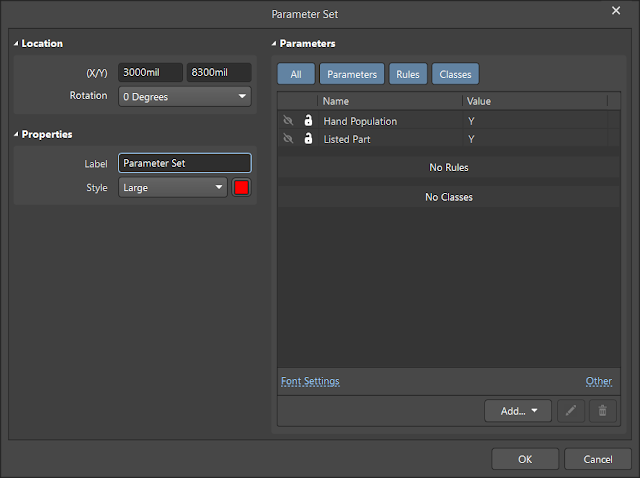
Example Altium Parameter Set

An additional custom parameter set for a ‘Listed Part’, was added to illustrate that multiple parameters could easily be added to the schematic as required.

Parameter Set in Bill of Materials
When generating the Bill of Materials (BOM) in Altium, details from the schematic parameter sets are available in the BOM Properties ‘columns’.
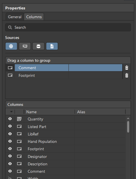
Altium BOM using Parameter Sets

Viewing the parameter set information in the BOM generated by Altium is possible by enabling the required parameter listed in the columns section of the BOM manager. This allows customisation of the various board fabrication or assembly houses.

Extract from Altium MiniPC Project with Parameter Sets

Pictured above is a portion of the generated BOM when the ‘Hand Population’ and ‘Listed Part’ parameter set entries were enabled.

For Altium projects that have several variants, components in schematics are likely to be controlled using the variants manager. Components are marked as fitted or not fitted. When a parameter set is used, the fitting of components with parameter sets in the BOM should be reviewed.

Sunday, 9 August 2020

Net Tie Application in Altium

Summary
This blog presents an example design employing a net tie component. Although Altium Designer was used to illustrate the net tie example, many existing packages support net tie functionality.

Existing Documentation
The Altium website contains examples for using net tie components, such as those listed on the page "Breaking the PCB Design Challenges with Net Ties". Developers support pages should be a readers the first destination when knowing that a net tie is required for a design.


Example
Initially, the requirement to use a net tie may not be apparent. In the example circuit below, a differential voltage measurement is required for an Analogue to Digital (ADC) device. For the purposes of this blog, the differential voltage measurement has negative connection of the ADC referenced to 0 V.  

The risk in connecting the negative ADC input, IN0_N, to the 0 V is the net name given to the pin. During routing of the board traces, the pin at the ADC input may be inadvertently tied to 0 V. Incorrect board routing can result in issues such as excessive noise floor voltages or inaccurate measurements not representative of the source (R1).

Example ADC Connections for Current Sensing without Net Ties
Using the example schematic with Altium defaults shown below, parts were placed on a Printed Circuit Board (PCB).


Example Altium Netlist Options

PCB Net
Net naming is shown in the capture below.

Altium Net Naming without a Net Tie, No Power Port Priority

Note that the 0 V net was renamed to ADC_Sig.IN0_N. 

Activating the power port priority checkbox in the Altium Netlist Options will ensure that the ADC_Sig.IN0_N net is renamed to 0 V. The net on the PCB appears as 0 V as shown in the capture below.

Altium Net Naming without a Net Tie, Power Port Priority

To retain the two separate net names, 0 V and ADC_Sig.IN0_N, a component is required to separate the nets.

Example ADC Connections for Current Sensing with Net Tie


For separating the nets, a net tie component is commonly used. Some designs may opt for a component such as a resistor with connected pads or thru-hole pad.

Altium Net Naming with a Net Tie, No Power Port Priority
A close-up of the net tie for the example is pictured below with side-by-side surface mount pads.


Rectangular Net Tie Component Close Up

PCB Net Tie
The capture below illustrates a surface mount net tie with exposed pads.


PCB Net Tie with Rectangular Exposed Pads

Net tie with solder mask covering pads.


PCB Net Tie with Rectangular Solder Masked Pads
 
Round net tie constructed of two semi-circle polygons

PCB Net Tie with Round Exposed Pad

Depending on the size and layout of the net tie component footprint, some PCB rules may require adjustment.


Rectangular Net Tie Component

For the rectangular net tie component shown above, the distance between the individual traces is greater than 0.254 mm.


Round Net Tie Component

The capture of the round net tie component above has a clearance violation using a standard clearance rule of 0.254 mm. PCB Clearance Rules should be configured to account for the proximity of pads or traces.

Final Thoughts
To preserve individual net names in a schematic which make a common electrical connection, the net tie component is a practical solution for PCB designers.

Alternatives to the net tie component include using a resistor, connector or abutting pads. The component pads are connected with traces, fills or polygons. For these solutions, PCB Clearance Rules should be configured to resolve resulting violations.

Thursday, 13 June 2019

PSoC5 Dual Application USB FS Bootloader

Summary
This post provides an example Cypress bootloader project which features dual bootloadable applications and updates through USB communications.

Why an Example
While looking into field upgrades for Cypress microcontrollers, it was found that the MiniProg3, Kitprog boards with snap off programming modules or a Cypress bootloader were commonly used in the example projects. This was no doubt a small portion of what is available but not what was required. Some examples featured a bootloader and a single application although none were published with dual applications.

Looking at the newer range of Cypress devices, there were dual application bootloader examples for the PSoC6 MCU however these examples were not portable back to the PSoC4 or PSoC5 devices.

Using a PSoC5 development board and related Cypress documentation, a project with basic bootloader and bootloader functionality was created.

Development Board
For this post the Cypress PSoC5 CY8CKIT-059 was used for testing dual application functionality. One hardware modification was made for detecting when USB power was applied to the Micro USB connector. The Micro USB connector is shown to the left side of the PSoC5 development board in the image below.


PSoC5 Test Setup
PSoC5 Test Setup
 
Bootloader Setup and Hardware Changes
The Cypress code example, USBFS_Bootloader.cywrk, served as the framework for the dual application project. 

As a first step the example projects reference PSoC device, CY8C3866AXI, was changed to a CY8C5888LTI-LP097 to suit the PSoC5 development board.

Opening the USBFS component the name of the USB descriptor string was changed under the String Descriptor tab to reflect the PSoC5 device.


USBFS String Descriptor Change
 
Under the Advanced tab of the USBFS component, the VBUS option was enabled. This input facilitates detection of USB power through a physical input on the PSoC5. Enabling the VBUS (input) in the USBFS component was not mandatory. The input serves two purposes, firstly the USBFS component can return the state of the USB power using the API - USBFS_VBusPresent(). Secondly the USB power (Micro USB connector) detection allows one possible method of initiating the Cypress bootloader when the device is bus powered.


USBFS VBUS Monitoring
 
With VBUS monitoring enabled in the USBFS component, an input was available on the component.
USBFS VBUS Monitor Input
 
As shown in the capture above, input P15_5 was connected to the component for USB power detection.

On the rear of the development board a wire link was made between the P15_5 pad and the Anode of component D2.


PSoC5 USB Bus to VBUS Input
 
Shown below is a portions of the PSoC5 development board schematic (Micro USB connector). The wire link connected from P15_5 to the Anode of D2 was made to ensure that USB (Micro USB connector) power was detected and not the power provided by the usual KitProg connector.


In the Bootloader component the wait for command was reduced to a time of zero so that the Application 1 or 2 could be called by the bootloader. The dual application and golden image support was also enabled. Golden image support was enabled in the Bootloader component to ensure that a valid Application 1 would always be available. It should be noted that the project will operate with only Application 2 programmed. Changes could be made in the firmware to prevent this operation.


Bootloader Component Configuration
 
A timer for flashing an LED and UART for debugging were also added to the project. These items were not critical for operation.

Bootloadable Setup
The bootloadable firmware (Applications) were essentially the same. These projects consisted of a Bootloadable component and each with a timer for flashing a LED. The difference between the two applications were the different LED flashing rates.


Bootloadable Component Configuration

For the settings in the Bootloadable component, it was stated on page 44 of the Cypress Bootloader and Bootloadable component datasheet that the Manual application image placement information for the dual applications should be the same.


Bootloader and Bootloadable Component Datasheet - Extract Page 44
The bootloadable dependencies (.hex and .elf) for the two applications was referenced to the projects bootloader.


Bootloadable Projects Bootloader Dependency
Bootloadable Projects Bootloader Dependency 
 
Bootloader Firmware 
For the Bootloader firmware, a check was added for the USB (Micro USB connector) power using the call USBFS_VBusPresent(). 

If the Micro USB power was detected then the Cypress Bootloader was initiated.
To update Bootloadable Application 2 over USB, a call using Bootloader_SetActiveAppInMetadata(0) was required.

Otherwise without Micro USB power the bootloadable applications were verified using the call Bootloader_ValidateBootloadable(). Switching to a valid Bootloadable application was made with application 2 taking precedence over application 1.

/**
* @file main.c
*
* @version 1.0
*
* @brief Shell example for Cypress Dual Application Bootloadable project                                      
*/

#include <project.h>
#include <stdbool.h>
#include <Bootloader.c>             /* Required to set active app in metadata */

CY_ISR_PROTO(SYS_TMR_HANDLER);
/**
* @brief System timer, flashes LED
*/
CY_ISR(SYS_TMR_HANDLER)
{   
    LED_Write(~LED_Read());
    Timer_2_ReadStatusRegister();
    isr_SysTmr_ClearPending();   
}

/**
* @brief Boot to valid APP2 then APP1 if no VBUS.
* @details VBUS present allow bootloader
*/
int main(void)
{
    CyGlobalIntEnable;
    isr_SysTmr_StartEx(SYS_TMR_HANDLER);
    UART_Start();
    USBFS_Start(0, USBFS_5V_OPERATION);

    if (USBFS_VBusPresent() == true)
    {
       LED_Write(true);
       Bootloader_SetActiveAppInMetadata(0);
       Bootloader_Start();
    }

    if (Bootloader_ValidateBootloadable(1) == CYRET_SUCCESS)
    {
        Bootloader_Exit(Bootloader_EXIT_TO_BTLDB_2); 
    }

    if (Bootloader_ValidateBootloadable(1) == CYRET_BAD_DATA)
    {
        UART_PutString("APP2 Bad");
    }
    if (Bootloader_ValidateBootloadable(0) == CYRET_SUCCESS)
    {
        Bootloader_Exit(Bootloader_EXIT_TO_BTLDB_1); 
    }

    if (Bootloader_ValidateBootloadable(0) == CYRET_BAD_DATA)
    {
        UART_PutString("APP1 Bad");
        Timer_2_Start();
    }    

    for(;;)
    {  
    }
}

Bootloadable Firmware 
For the Bootloadable applications the firmware was made the same. To differentiate between the active applications the flashing LED rate was set for 1s in Application 1 and 2s for Application 2. A compare value in the Timer (System) component was used to configure the flash rate. 

/**
* @file main.c
*
* @version 1.0
*
* @brief Shell example for Cypress Dual Application Bootloadable project                                      
*/

#include <project.h>
#include <stdlib.h>
#include <stdbool.h>

CY_ISR_PROTO(SYS_TMR_HANDLER);
/**
* @brief System timer, flashes LED 2 sec
*/
CY_ISR(SYS_TMR_HANDLER)
{   
     LED_Write(~LED_Read());
    Timer_2_ReadStatusRegister();
    isr_SysTmr_ClearPending();   
}

/**
* @brief Init PSoC
*/
void PSoC_Init() 
{                                                             
    Timer_2_Start();
    isr_SysTmr_StartEx(SYS_TMR_HANDLER);                                                   
}

/**
* @brief Handle main
*/
int main()
{        
    CyGlobalIntEnable;
    PSoC_Init();
    for(;;)
    {                         
    }
}


Bootloadable Firmware Build
Other than selecting Build All Projects from the Build menu in PSoC Creator, no other changes were required. Following a successful build process, several files are generated. For this blog the project was built in Debug with relevant .hex and .cyacd files located in the location \CortexM3\ARM_GCC_541\Debug.

Bootloader Firmware Testing 
To test the Bootloader only the Bootloader application was programmed into the PSoC5 development board. 

Running standalone and without the USB (Micro USB) connected, the serial debug returned the string "APP2 Bad" followed by "APP1 Bad". With no valid application detected the onboard LED was flashed at a fast rate courtesy of system timer.

With the KitProg disconnected and the USB (Micro USB) connected the Bootloader set the onboard LED to ON and started the Cypress Bootloader.

To test programming of the Bootloadable application the Bootloader Host application, from the PSoC Creator Tools menu, was launched. This application provided the interface for updating Application 2; Application 1 was marked as a Golden Application and cannot be updated even if it is not programmed.


Cypress Bootloader Host Application with USB Connection

The Bootloader Host application indicated the Active Application in the top right hand corner of the window. Attempting to program the relevant .cyacd file for Application 1 resulted in an error relating to the active application as shown in the capture below. Application 1 was marked as the active application by the Bootloader using the call Bootloader_SetActiveAppInMetadata(0). 

Modifying the code to switch between the active applications should be possible.


PSoC Application Marked Active Message

  Attempting to program Application 2 with Application 1 results in a checksum error message as shown below.


Programming PSoC Application 1 onto Application 2 Message

  While programing Application 2 with the relevant file, App2_2.cyacd is possible and programming is successful, there is no relevance as this is a dual application project with a golden Application 1.

Bootloader with Bootloadable 1 Firmware Testing 
For the following sets of tests the Bootloader and Bootloadable Application 1 was programmed into the PSoC5 development board.

Running standalone and without the USB (Micro USB) connected, the serial debug returned the string "APP2 Bad". With Application 1 returned as valid the application is started. To validate operation of the application, the onboard LED was flashed at a rate of 1 sec ON then OFF.

As with the initial Bootloader test, the KitProg was disconnected and the USB (Micro USB) connected. The Bootloader set the onboard LED to ON and started the Cypress Bootloader.


Again launching the Bootloader Host from the PSoC Creator Tools menu provided the interface for updating Application 2; Application 1 was marked as the Active Application.

Programing Application 2 with the relevant file, App2_2.cyacd, was completed without error.

PSoC Application 2 Programmed Message

  After cycling the power to the development board, Application 2 was detected as a valid application by the Bootloader and was started. The onboard LED was flashed at a rate of 2 sec ON then OFF.


Project Uses
The proposed implementation in this project may be useful for designs where a minimum operating firmware is required for a product or design. This minimum operating firmware would be considered the Golden application version. A dual application with a Golden application also addresses the issue of application corruption during download, although this event is possible although unlikely.

A further application for a dual application project may be in a commercial product environment. Consider that a commercial product may require end to end device testing which requires a separate firmware implementation to function with a test environment. With modification of the firmware to select applications, a dual application project could allow for execution of either firmware thereby minimising reprogramming.

Some limitations of this project implementation relates to the increased use of memory space and the need to provide specific Bootloadable applications. These applications must occupy the memory locations as defined by the Cypress documentation and project software.

Downloads
The PSoC Creator 4.2 project for the example in this blog was saved as a minimal archive.

USBFS Bootloader with Dual Bootloadable Applications

Saturday, 25 February 2017

Cypress PSoC VT100 Code Example

Summary
As an alternative interface to one of my projects, basic VT100 functionality was implemented across serial (USB) on a Cypress PSoC4 BLE device. The Cypress iprintf code was used with a wrapper to implement basic VT100 features.

The screen capture below shows basic control of text and colour.

VT100 Example in TeraTerm

As a starting reference the
Bash Hackers website was used for the VT100 escape codes. A plethora of information can be found at sites such as Technopedia, TermSys, NorthEastern Uni, ASCII-Table and ISP to name a handful. What has been provided is only a portion of the total VT100 commands available.

Code for the PSoC
For Cypress Creator development environment a separate VT100 source and header file were created with the necessary escape commands.


VT100 Commands
VT100 Commands
Foreground and background colors.


VT100 Colours
VT100 Colours

Cypress already provide a PSoC Creator example project with iprintf, which works effectively as the low level interface. A reference to this library was included in VT100 code.

To use a number of commands at once or to configure the location of the cursor a few functions were written, prototypes below. There is room to improve these functions but for testing they function as required.


VT100 Function Prototypes

Usage in the software main shown below.

VT100 Example Usage
VT100 Example Usage


Testing
Testing was also performed with other terminal packages such as PuTTY and RealTerm.

VT100 Example in PuTTY (Windows)
TermPuTTY under Ubuntu Mate, customised settings

VT100 Example in PuTTY (Ubuntu Mate)

RealTerm was placed in ANSI mode with good results, except for the colours.

VT100 Example in RealTerm

Downloads


vt100.c
vt100.c

vt100.h
vt100.h


Change Summary

Version 1.02 (15 March 2017)
  • Added GPL details
  • Corrected two text command enumerations
  • Updated PSoC Creator project
Version 1.01 (11 March 2017)
  • Added defines for background colour
  • Changed names of foreground colour defines
  • Updated PSoC Creator project
Version 1.00 (26 February 2017)
  • Created PSoC Creator project for initial vt100 commands