Thursday, 31 August 2023

PCB Mouse Bites and Board Traces

Introduction 
This blog shows testing of
circuit board mouse bites that have copper traces passing through them. The breaking strength of the mouse bite was also measured during testing.

Mouse Bite Test Boards

Mouse Bites
The use of mouse bites with circuit boards can be as varied as the application however, some common examples of applications include board panelisation, tooling strips, test coupons, in-circuit testing or breakaway boards. This blog’s focus is on small breakaway boards commonly used in embedded programming or development boards where traces are routed through the mouse bites.

SparkFun published a white paper in 2022 (Author, Nick Poole) that illustrated testing of various mouse bite combinations. The paper from SparkFun serves as a good reference for designer as it details the combinations and the force required to break the board under test (mouse bite).

This blog performs similar tests to those conducted by SparkFun however, the intent was also to see the effect of circuit board traces after breaking the mouse bites.

Test Board
A circuit board was created with four mouse bite configurations. The drill hole sizes varied between 0.38 mm to 1.00 mm. The pitch between holes was adjusted to suit the drill size and test boards.

Test Board for Mouse Bites

Between the holes of the mouse bites, traces were routed either externally (top and bottom) or internally traces (two mid-layers). This created eight combinations of trace and mouse bites for testing.

3D View of Test Board for Mouse Bites

Measurements
For each mouse bite break measurement, a simple setup containing an attachment to the test board and connecting wire to a digital scale was used.

Mounted Test Board

Measurement Tool
Measurement Tool

Results
The table below lists the test number against the mouse bite drill size and pitch combination. 

Mouse Bite Configurations

As seen in the chart below, there was little difference in test results between the various mouse bite configurations and lifted board traces. External board traces on average lifted on the opposite side of the circuit board. Any lifted traces were considered damaged. No internal traces were seen to be damaged.

Type vs Listed Traces After Testing

The chart beneath shows the average measurement (kg) required to break the mouse bite boards. A notable difference in the last two tests was expected because of the larger mouse bite holes meaning less circuit board material.

Measurements for Breaking Mouse Bites
Type vs Measurements for Breaking Mouse Bites

The edge view of the main board in the image below shows the different breakage patterns.

Circuit Board Edge with Mouse Bites Removed

During two measurements, the test board broke cleanly except for one layer that lifted and tore away from the main board; as shown in the picture below.
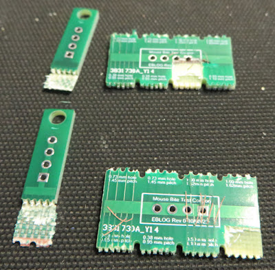
Damaged Test Boards
Damaged Test Boards

Summary
The results in this blog with the specific test board indicate that internal traces experienced fewer issues with lifted traces. Other combinations of routing such as using a single side for external traces will likely be effective.
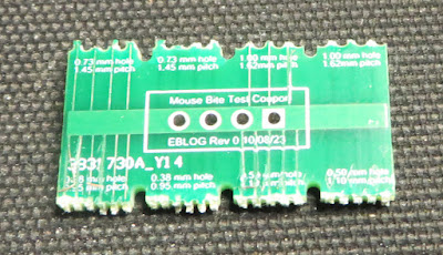
Mouse Bite Test Piece

For designs only requiring mouse bites in a circuit board design, most hole-pitch configurations are useable although the overall design should be reviewed as part of Engineering practices.

Sunday, 9 July 2023

Risinglink PD201W Power Failure Detector

Introduction
This blog provides a teardown of the Risinglink PD201W Power Failure Detector and wall plug adaptor.

Risinglink Module
Risinglink Module

Power Failure Detector Supplier
The power failure detector is branded with the logo of the company Risinglink. There are no product specifications for the detector on the Risinglink website but documentation is provided with the detector when purchased.

Package Contents
A mains wall plug (USA), USB cable and documentation are shipped with the power failure detector shipment.
Opening the Detector
A thin flat bladed screwdriver was used to release the lid from the case. The joint near the R and K in the Risinglink logo was the optimum lid leverage position. The plastic lid has two clips to retain the lid in the housing.

Risinglink Module Internal

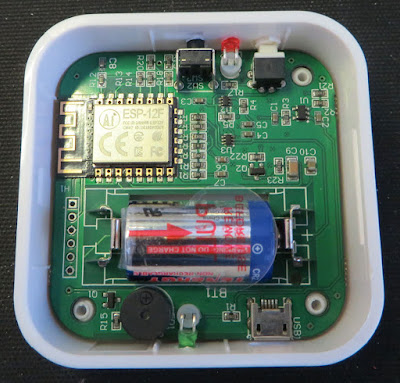
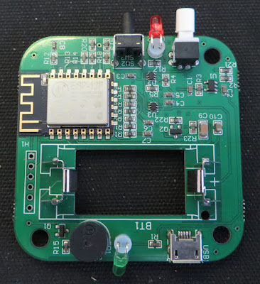
The ESP-12F WiFi module, CR2 battery, buzzer, switches and LEDs are immediately visible on the circuit board upon opening the unit. Removing the circuit board was possible by pressing the green LED away from the edge of the case. There are no components on the bottom side of the circuit board.

Risinglink Circuit Board


The battery manufacturer’s website (Tenergy) shows that the battery cell has a capacity of 800 mAh (Lithium). 

According to the ESP datasheet, operating the WiFi at continuous transmission draws an average of 71 mA. This would theoretically mean that a fully charged battery could monitor the status of the mains for hours.

As detailed in the documentation shipped with the detector, the white switch powers the detector with visual feedback provided by the red LED.

The black pushbutton is used to change operating modes as required when configuring the detector.

For the USB connector, only the power connections are utilised for monitoring the mains. No USB communication is possible to the detector. USB power is indicated through the illumination of the green LED.


Email Details
Notification emails are sent with “via amazonses.com” in the address. Emails events are received on the initial start-up, when a power outage occurs or when power restoration is detected.

The device PowerDetector started. Below is the device status at 01/01/2023 12:00PM.

  • Power Status: ON
  • Battery: 100%
  • WiFi Signal: -51

As mentioned in the documentation, an email is sent after 24 hours if there is no communication with the module.

The device, ............, may be OFFLINE. No ping from the device within 24 hours. Please check WiFi connection, Internet service, etc. Please contact support@...... if any question.

Wall Plug
The wall plug (model HNT-H510) features an internal On-Bright controller responsible for the control aspect of generating DC 5V in either Constant Voltage (CV) or Constant Current (CC) mode. As the image from the wall below shows, the design is the usual compact solution.

Wall Plug Internals
Wall Plug Internals

ESP-12F
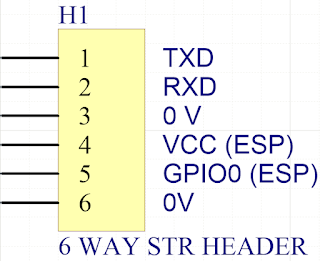
On the detector circuit board is an unpopulated 6-pin straight header (H1). Using the datasheet of the ESP-12F and a multimeter, the pinouts of the header were determined as displayed in the image below.

Pinouts for RisingLink Connector
Pinouts for Risinglink Connector

A TTL to USB converter was connected to the header pins Tx, Rx and 0 V. An oscilloscope was used to measure the transmitted UART data bit time which was approximately 13.3 ms or 75 bps during bootup. Data was shown however this was not reviewed in further detail. Programming information for the ESP can be found on dozens of sites, on example here.


Example data on boot.
ets Jan  8 2013,rst cause:4, boot mode:(3,7)
wdt reset
load 0x40100000, len 30596, room 16
tail 4
chksum 0x3e
load 0x3ffe8000, len 2004, room 4
tail 0
chksum 0xa1
load 0x3ffe87e0, len 4752, room 8
tail 8
chksum 0x6a
csum 0x6a


Modifying the Power LED
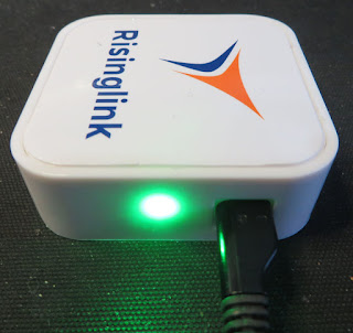
Situated on the side of the detector housing is a green LED. When a 5 VDC USB power adaptor is connected, the green LED bursts into operation. The brightness of the LED may be beneficial for a large factory but for a confined space, the LED brightness may benefit from a reduction.

Bright LED on Risinglink Unit

The green LED uses a 1 k 0603 current limit resistor, R1. 

Resistor R1 on Risinglink Unit

To reduce the brightness of the LED, resistor R1 was increased to 10 k with the effects shown below. Resistor R1 was located between the green LED and the USB connector as shown in the capture above.

Dimmer LED on Risinglink Unit

 
Final Thoughts
The Risinglink PD201W is reasonably designed and simple to use. An option to use a custom email client over Amazon services would be preferable, especially for clients needing to security harden their network. 

Additionally, a helpful upgrade to the detector could be a battery-only access panel or a rechargeable battery.

Saturday, 24 June 2023

Model Rocket Launcher WiFi ESP8266

Introduction
This blog follows the redesign and development of a model rocket launcher controller that features WiFi communications to control the launch process. This design uses an ESP-based microcontroller module. The Arduino platform was chosen for code development.

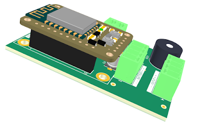
Rocket Launcher 3D Model

Redesign
To control the launch in the previous model rocket launcher design, Bluetooth communications were used between a PSoC microcontroller and an Android phone. The interface was changed to WiFi to remove the need for developing a phone application. Controlling a rocket launch through WiFi would be independent of a phone or computer operating system.

WiFi Module
For the launcher redesign, an off-the-shelf ESP module capable of WiFi was chosen from Adafruit. The ESP module was chosen for a few reasons. Firstly, the module’s price was relatively low (USD 10). The module was readily available compared to other dedicated microcontrollers. Lastly, using an ESP module meant that the rocket launcher design could be migrated more easily to other ESP devices.

Adafruit Huzzah ID 2471 (Courtesy Adafruit)

Reused Design
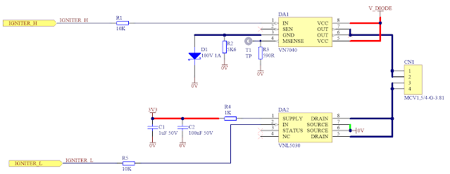
The same section of circuit responsible for driving the rocket engine igniter was taken from the previous design. This section consisted of high (VN7040) and low-side (VNL5030) switching drivers (ST Microelectronics).

Rocket Launcher Igniter Drive Circuit

Circuit Updates
To begin the schematic update process, the ESP module was created in the schematic libraries. The new part replaced the previous PSoC microcontroller and associated circuitry.

The Altium PCB model was downloaded from the website SnapEDA.

Capture of Adafruit Huzzah PCB Footprint from SnapEDA

Schematic Updates
On the ESP module schematic page, the power supply connections and ST driver control signals were mapped to the ESP.

Rocket Launcher - Huzzah Circuit Connections

Audible notification of an impending launch was retained using the buzzer. Connections were mapped to the ESP.

Rocket Launcher - Buzzer


The display (LCD) was infrequently used in the previous design so it was removed and replaced with an LED.

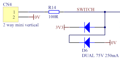
The launch button input to the ESP module was retained for testing purposes.

Rocket Launcher - Optional Launch Button

Connections were made to ESP module pins that had no special functions.
 
Output Drivers

Schematic changes were made to the ST output driver’s power supply. This was required to match the ESP module’s DC 3.3 V supply voltage. The feedback monitoring from the ST drivers was removed from the design because of the reliable performance of the ST drivers.

Power Supply
A DC-DC step-down converter was retained for the power supply. Texas Instruments part LMR50410 featuring an integrated diode was selected to replace the previous DC-DC converter.

Another benefit of the DC-DC converter is its operating voltage which is wider than the ESP modules linear regulator (LDO). The LDO has a maximum rated input voltage of DC 6 V. This voltage does not suit all battery chemistry types.

Rocket Launcher - Power Supply

Battery voltage monitoring using the ADC on the ESP through a resistor divider was kept for experimentation and possible future use.

Circuit Board
There were no caveats defined for the shape of the circuit board (PCB). The placement of components drove the PCB shape. Minimal design constraints for the PCB meant that the PCB was set up for components on both sides.

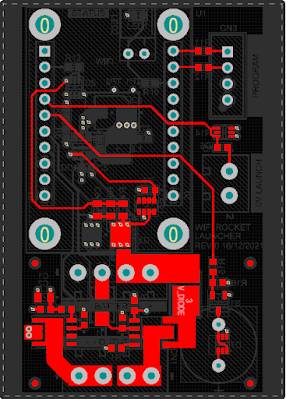
The capture below shows the PCB top layer with the ESP module, power supply underneath the ESP module, buzzer and optional screw terminals. To fit the power supply beneath the ESP module, pluggable headers were utilised to space the ESP module off the board.

Rocket Launcher PCB - Top Layer

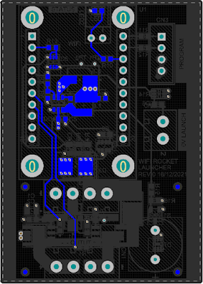
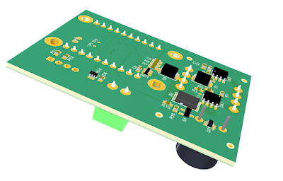
The next capture below shows the PCB bottom layer containing the output switching drivers and related components.

Rocket Launcher PCB - Bottom Layer

Four PCB layers were used for the launcher board stack-up. Captures of the two internal power planes have not been shown.

After component placement and routing, the board size reached a comfortable size of 62 x 44 mm. On the longest PCB axis, a set of 3 mm strips were added to suit mounting in an enclosure. Pictured below is a 3D side and rear view of the board.

Rocket Launcher - 3D Side View
Rocket Launcher - 3D Rear View

In part 2 of the launcher blog, the PCB construction and initial testing will be performed.

Wednesday, 31 May 2023

Circuit Board Return Path Via Placement Options

Introduction
This blog discusses a few options that new circuit board designers may use for return path vias as a result of signal traces changing circuit board layers through using vias.
 
Further Literature

It is highly recommended that existing content from industry figures such as Eric Bogatin or Rick Hartley are reviewed. Related circuit board information is available from YouTuber channels such as Robert Feranec or Phils Lab to mention a few.

PCB Routing Example
For circuit board designs that feature microcontrollers, microprocessors, FPGA or similar devices with high pin count or spacing density the existing connections to power rails through vias can serve as return paths. In the image below, taken from the Altium Mini-PC board, the green highlighted vias indicate the several 0V (GND) power connections that may function as return paths for the DDR memory address, data, clock and control signals.

Altium Mini-PC Board Highlighted GND (0V) Vias (Courtesy Altium)
 
Reducing Return Path Distance
The capture below is a further extract from the Mini-PC demonstration board showing a distance measurement between a return via and a differential DDR clock pair.

A Texas Instruments Application Note, High-Speed Interface Layout Guidelines, 2023 states that the signal to return via distance should be a maximum distance of 5 mm (200 mil) although that value could be considered design dependent. For the Mini-PC demonstration board, the distance between the return via and differential pair is small, some 2.1 mm.

Altium Mini-PC Board Differential Via Pair (Courtesy Altium)

Consider a situation where the return path distances needed to be reduced. On the Mini-PC board, a smaller distance could be achieved following a circuit board review. Traces on the layers could be moved to make room for a via closer to the differential via pair. The capture below shows one possible change with a reduction to 1.4 mm.

Altium Mini-PC Board with Closer Return Path Via (Courtesy Altium)

Board Space Limitations
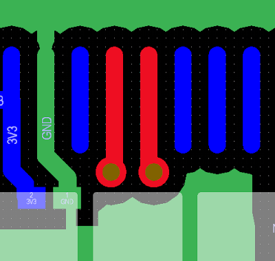
A more common limitation when adding or altering return path vias could be related to circuit board space. In the example below, the traces in the red colour identify a differential pair. There is no return path via in close proximity. The while highlighted rectangles represent pads on the other side of the circuit board.

Differential Pair with No Return Path Via on a Double Sided Circuit Board

The reason for no return path via in the area is two-fold. On the opposite side of the circuit board is a surface mount component with large pads making return via placement difficult. The second limitation is due to the PCB rules. The smallest via hole size is configured for 0.3 mm.

The limitation created by the component on the opposite side can be overcome using a number of solutions. Using the existing circuit board via the size of 0.3/0.5 mm (via hole size/via diameter) three vias could be placed onto the circuit board as shown below. This solution yields a differential pair to return path via distance of 2.3 mm.

Differential Pair with Three Return Path Vias on a Double Sided Circuit Board

Differential Pair with Three Return Path Vias on Other Side of Circuit Board

Another solution to consider is changing the board design rules. The circuit board clearance rule could be reduced from 0.2 mm to 0.15 mm since the smaller clearance is supported by many fabrication houses. 

Paired with the board clearance change, the via hole size could be reduced. For instance, a via of hole size and diameter 0.254/0.444 mm could be selected. In regards to capabilities, circuit board fabrication houses can manufacture smaller via hole/diameter measurement of 0.15/0.28 mm (drilled). Applying the two changes mentioned in this section, a via can then be placed less than 1 mm from the differential pair.

Differential Pair with Single Smaller Return Path Via on a Double Sided Circuit Board

No Space or Other Limitations
For some board designs, it may be impractical to place a via close to a signal that requires a return path. Should board space and routing permit, via stitching throughout the board or a via shielding around the board or relevant section of the circuit may be alternative solutions.

Example of Via Stitching on a Circuit Board

Example of Via Shielding on a Circuit Board

Summary
Even though the placement of return path vias may be a semi-automated process with some software design tools, the lack of circuit board space to position vias in optimum locations still vexes novice and experienced board designers alike. This blog puts that other solutions may be found by reviewing the nominated fabrication house’s manufacturing capabilities and the minimum manufacturing circuit board requirements.