Saturday, 31 July 2021

PCB Solder Jumper Pads

Summary
This blog summarises the tests performed on a selection of Printed Circuit Board (PCB) solder (bridge) jumpers. PCB jumpers are frequently found on PCB's used in electronic equipment. For testing, jumpers were reproduced on a single PCB in various sizes for comparison and testing purposes.

Solder Jumper Test PCB

Solder Jumper
The PCB solder jumper electrically connects two, or more, separate circuits. The function of the solder jumper performs is as varied as the type of jumpers seen on electronic equipment.

Solder Jumpers on LCD PCB

Solder Jumper Design
Some of the early solder jumper designs were novel as two or more pads places relatively close to each other, consider an 0201 style footprint. Either a blob of solder, a soldered zero-ohm link or a short piece of wire was required to join adjacent pads.

Some websites have entire pages dedicated to PCB jumpers for CAD packages such as Eagle.

Example Eagle PCB Jumper Design
 

The technique of using two pads is still widely used however, there have been some variations to the solder jumper design. For example, the forum posts on DIP Trace show four alternative jumper designs.

Changes in the solder jumper design have been a result of improving manufacturability, reliability when reworking the jumper and in some instances a general reduction in the footprint size.

For example, changing the two side by side pads, think of an 0201 resistor, to a chevron (arrow) or pad in pad can increase the mating area between the two solderable surfaces. An increased surface area can result in a better chance of solder adhesion. The adhesion can be important for boards that are run through reflow soldering.


Solder Jumper Prototyping
Some of the PCB jumpers depicted in this blog were replicated on a test panel. The focus of the prototyping was for small to miniature solder jumpers.

Unsoldered Jumper Test PCB

Only J11 has a minimal solder mask between the jumper pads.

PCB Arrow Solder Jumper
PCB Arrow Jumper

J1 and J2 represent the arrow jumper which was created in a nominal and miniature size.


PCB Tongue and Groove Solder Jumper
PCB Tongue and Groove Jumper

J3 and J4 represent the jumper design seen on portable/wearable electronic equipment. Two very small jumpers were created.


Various Ball and Socket Solder Jumpers
Various Ball and Socket Jumpers

J5 through J10 were designs similar to those presented on DIP trace with a few personal variants using a pad inside a pad.

Large Small Pad Solder Jumper
Large Small Pad Jumper

J11 was a design mentioned on an Engineering blog where a larger pad with more solder was more likely to bridge to a smaller pad.


Side by Side Pad Solder Jumper
Side by Side Pad Jumper

J12 was a common design used by the Open Source forums for Arduino shields, OLED or LCD boards.

Dual Round Pad Solder Jumper
Dual Round Pad Jumper

 J13 was created to test round pads side by side.

Four Pad Solder Jumper
Four Pad Jumper

J14 was inspired by the LCD to test a variant of inward facing arrows.

Testing Solderability
A 1.2 mm chisel tip (Hakko T12-D12) with lead-free solder was used to bridge the solder jumpers. As shown in the image below, not all jumpers (J2, J4, J11 and J13) would bridge using the chisel tip.

Chisel Tip Soldered Jumper Test PCB

The same chisel tip was used to remove the solder bridges. For most of the solder jumpers, the solder was removed in one pass. All jumpers were tested for continuity, none were shorted.

Chisel Tip Desoldered Jumper Test PCB

For a second test, a 1.0 mm 45 degree conical tip (Hakko T12-BC1) with lead-free solder was used to bridge the solder jumpers. Again not all jumper (J2 and J4) would bridge with the conical tip.

Conical Tip Soldered Jumper Test PCB

Desoldering jumper with only the 1.0 mm conical tip was time-consuming due to the small amount of solder removed in each pass. Desolder braid was required to remove enough solder from the jumpers in a single pass. Alternatively using a 3.0 mm 45 degree conical tip (Hakko T12-BC3) allowed cleaning of the jumpers without desolder braid.

As a third test with reflow soldering, solder paste (NC 254 SAC 305) was applied to the PCB manually.

Solder Paste Application on Jumper Test PCB


The result of the reflow process was that the smallest solder jumpers, J2 to J4 and J11 and J13 formed a bridge. Any soldering iron tip could be used to remove the bridge. Larger pads did not bridge likely due to the pad size and small amount of solder paste.


Reflow Solder Result on Jumper Test PCB

Summary
For testing in this blog, soldering iron tips in the form of chisel, conical and different 45-degree were used.

Using the metrics of solderability and ease of desoldering, jumpers J5, J7 and J12 worked with all the types of soldering iron tips.

The smaller jumpers, J2, J3 and J13 required a small tip for reliable production of a solder bridge during hand soldering.

Jumpers J4 and J11 did not solder reliably using hand soldering however reflow soldering was successful in all three attempts.

Larger jumpers J1 and J4 together with the multi-pad jumper J14 required larger soldering tips for creating the solder bridge. These jumpers were not tested extensively with reflow soldering.

Some of the jumpers detailed in this blog are found in hobbyist or consumer equipment with each designed to suit their application.

To suit the home hobbyist, jumpers J1, J5 or J12 would be ideal choices.

Finally, a note concerning PCB production. The smallest jumpers with small pads and 0.1 mm pad to pad spacing significantly increased the cost of the PCB; a salient point when moving to miniature or high-density PCB designs.

Downloads
Gerber files downloadable using the link below.

Jumper Gerber Files
Jumper Gerber Files


Sunday, 27 June 2021

Failing B22 E27 LED Bulbs

Summary
This blog reviews E27 or B22 style LED bulbs and the heat produced during operation.

LED Bulbs
In many mains powered LED bulbs a non-isolated, AC to DC LED driver is central to the design. For some bulbs, the Printed Circuit Assembly (PCA) containing the LED driver is separate from the LEDs. The LED
Printed Circuit Board (PCB) is usually metal backed to assist in heat dissipation. Both the LEDs and driver assemblies generate heat however the majority of heat is generated by the LEDs. 

Failed LED Bulbs
After several LED bulbs failed
across a period of weeks whilst daytime temperatures were high, the bulbs were opened for investigation. A failed Surface Mount (SMT) LED on the PCA was easily identified by black dots. Other LED bulbs had failed controllers.

Single Failed LED (Black Dots)


LED Testing
The LED driver on the bulbs was identified from the manufacturer Bright Power Semiconductor. The manufacturer datasheet detailed the LED driver‘s
single string capability was 120 mA with a maximum string voltage of DC 72 V.

Based on the driver string voltage, current with the dimensions of the LED in the bulb, the LED manufacturer appeared to be Everlight however this is not substantiated.

Using the specifications of the Everlight LED as a reference; a forward voltage of 9.15 V and 100 mA maximum current, a single LED board was left on the board. The single LED was powered from a benchtop power supply and measurements were taken.

For a constant current of 100 mA, the forward voltage was approximately 9.1 V. Measuring the temperature of the single LED after 15 min showed the case temperature of the LED reached 85°C mounted against the metallised board.

Temperature of LED Case

The rear of the metallised board reached nearly 40°C in the open air. When installed in the bulb, the temperature of the metallised board is expected to be higher considering the enclosed space.

Temperature of LED Rear Side
 
Changing the power supply to constant voltage mode with a 125 mA current limit, several measurements were performed at different voltages. Temperature measurements were also performed with a 26°C ambient. The graphed results are illustrated below.

LED Temperature vs Forward Current

Summary
During the testing process in this blog, a maximum LED case temperature of 101°C was measured with an ambient of 26°C.

Highest LED Temperature

It should be noted that many LEDs will operate continuously with a junction temperature at or above 100°C. Manufacturer datasheets usually provide graphs showing luminous flux changes with temperature which help determine derating performance.

The derating of luminous flux versus temperature varies considerably between LED manufacturers.
For the LED described in the blog, which was suspected to be manufactured by Everlight, the maximum junction temperature was 115°C. The derating curve to 115°C is shown below.

Everlight Luminous Flux vs Temperature

Using the bench tests results from this blog, it would be anticipated that with all LEDs active and an ambient temperature over 40°C, the LED junction temperature would exceed the datasheet rating. 

LED Bulb Driver and LED PCA's Showing Heat Discolouration

Interestingly many over the shelf LED bulbs do not detail maximum operating temperatures on their packaging or datasheets. For the LED bulb described in this blog, the high generated temperature was likely a contributing factor to the reduced lifetime of the bulb.

Friday, 14 May 2021

WaveDrom with Confluence (Server)

Summary
This blog illustrates how Atlassian's Confluence tool can work with WaveDrom to render scripts. The process requires
Confluence Administrator access and a small amount of configuration.

Example of WaveDrom Output

Enabling the HTML Macro
The process of enabling HTML Macro's in Confluence Server is documented in this blog and formally on the Atlassian website here.   

The Custom HTML feature is accessed under the Administration 'cog' icon.

Confluence Manage Apps

Open the Manage Apps item. Select System from the drop-down list box. Type HTML into the Filter Visible Apps text box.

Confluence Locate HTML Macro
 

After typing into the filter, the HTML Macro should be displayed.

Confluence HTML Macro


Expand the Confluence HTML Macro heading.

Confluence HTML Macro Expanded

Then expand the modules enabled heading.

Confluence HTML Macro Enabling


Locate the html (html-xhtml) entry and enable.

This first step is complete.

Custom HTML
To execute a WaveDrom script, the Confluence HTML Macro is processed by custom code added to Confluence pages. The custom code links  JavaScript libraries and calls a function to process the WaveDrom script.

Information relating to the libraries is detailed under the Web Usage section of the WaveDrom site on GitHub.

Below is the code taken from the GitHub site.

<script src="https://cdnjs.cloudflare.com/ajax/libs/wavedrom/2.6.8/skins/default.js" type="text/javascript"></script>
<script src="https://cdnjs.cloudflare.com/ajax/libs/wavedrom/2.6.8/wavedrom.min.js" type="text/javascript"></script>
<
body onload="WaveDrom.ProcessAll()">

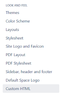
To add Custom HTML, open the Custom HTML entry under the Look and Feel heading whilst under Confluence Administration.

Confluence Custom HTML

Click Edit.

Confluence Added WaveDrom Link

Under the End of Head section, add the code from the GitHub site.

Confluence Adding WaveDrom

Click Save, this step is completed.

Note that some companies or IT providers may have policies restricting access to external sites.

HTML Macro on Pages with WaveDrom
A script can be generated in the
WaveDrom editor then copied into Confluence after it has been finalised or the script can be manually entered into the a HTML macro.

An HTML macro is required to contain the WaveDrom script.

On the required page, use the Insert More Content (Ctrl + Shift + A) to locate the HTML macro. Typing HTML into the Search box will expedite the process.

Confluence Select Macro

Click the HTML then Insert.

Confluence Select Macro Insert

An editable box titled with HTML be displayed.

HTML Macro Inserted into Confluence
 

The WaveDrom script is then copied into the HTML field.

HTML Macro with WaveDrom Script

Click Update at the bottom of the Confluence page to complete the change.

View the page to ensure the render has worked.

Example of WaveDrom Output

Final Thoughts
Tools such as WaveDrom can provide a permanent description of information such as timing diagrams. Integrating the functionality of WaveDrom into a collaboration tool such as Confluence can reduce the requirement for separate applications and documentation tool consistency.


Thursday, 29 April 2021

Novel Voltage Interruption Tester for IEC 61496-1

Summary
This blog provides details of a novel voltage interruption tester that demonstrates the requirements listed in the IEC 61496-1 standard, section 4.3.2.2. 

The tester was needed because certain types of electronic hardware must be tested to the IEC 61496-1 standard and dedicated testing facilities have had reduced access during the pandemic. The purpose of the tester in this blog is preliminary testing which would not replace an authorised testing facility.

Description
The interruption test hardware described in this blog was designed for DC systems to 48 V and currents to 3 A. For design constraints, interruption timing was considered important, followed by access to available hardware then output voltage regulation.

The capture below displays section 4.3.2.2 of the IEC standard which shows the timing of the three interruption tests.

Supply Voltage Interruptions

Hardware Solutions
Off the shelf power supply evaluation boards such as the Vishay SiC461 were tested initially. To control the output voltage, a programmable resistor replaced one of the feedback elements. By using a programmable resistor, a 10 ms pulse width was achievable. However, the output voltage rise and fall times were asymmetrical and several milliseconds in duration.

Alternative solutions utilising linear regulators such as the LM317T were analysed. The linear regulator produced very sharp output voltage rise and fall times. The limitation of the linear regulator was the LM317 voltage regulation and accompanying device heat dissipation.

By utilising existing resources, such as individual benchtop supplies, a simpler solution was identified. It was likely that workspaces would have access to one dual output or two single regulated adjustable power supplies. These supplies could be used together for the switching tests.

The hardware in the system consisted of a microcontroller (PSoC) that interfaced to a pair of optocouplers (4N28) in turn driving two high-side switches (BTS50085). The output of each high-side switch was tied together with series diodes (1N5404) to produce the output.

One design weakness using this solution was the supply to output voltage drop. As the cumulative voltage drop of the high-side switch and diode changed with load current, the power supplies required adjustment to achieve the correct test voltages.

Hardware Concept
Shown below was the original concept proof of the hardware. The high-side switch datasheet lists an operating voltage to some 58 V and a current of 11 A.

Interruption Tester Concept Hardware


Circuit Overview
Control signals generation was performed by a microcontroller; any type could perform the task as the signals are slow-moving. Two control signals from the microcontroller drive a set of optocouplers. For this design, an ancient pair of 4N28’s were fitted. 

The transistor output of the optocouplers switched the high-side driver inputs to 0 V. This was required as the inputs of the high-side drivers BTS50085 must be switched to 0 V to activate their outputs.

Microcontroller
An off the shelf CY8CKIT-059 Cypress development board implemented a PWM to drive two outputs for the optocouplers. 

The onboard switch and LED acted as the user interface. 

Repetitive switch presses selected a subsequent test. Flashes from the onboard blue LED indicated the test number. No flash for off, one flash for test one up to three flashes for test three.

For the top design in PSoC Creator, the first PWM output provided the timing for the voltage dip. The second PWM output configuration and some flip flops ensured that the half voltage was active before and after the first PWM changed state. Understandably there are other ways to use the PWM component, again this was a concept proof.

PSoC Creator PWM Test Setup

The PWM was configured as illustrated below. Settings were controlled from within the code.

PWM Component Setup
PWM Component Setup


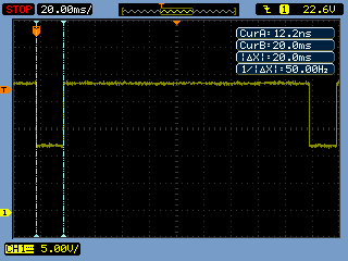
The rise and fall times (10%, 90%) were 20 us and 90 us respectively
with the output driving a resistive load.

Rise Time for Resistive Load

Fall Time for Resistive Load

Output Waveforms
The following captures were taken when driving a resistive load.
 

Interruption Test 1 with Resistive Load
 

Interruption Test 2 with Resistive Load


Interruption Test 3 with Resistive Load

The next captures were taken when driving a DC 12 V fan.

Interruption Test 1 with DC Fan

Interruption Test 2 with DC Fan

Interruption Test 3 with DC Fan

Output Voltages
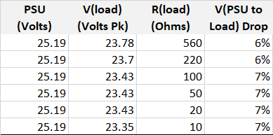
For the three interruption tests, various loads were tested and peak voltages measured.

Interruption Test 1 with Various Resistive Loads

Interruption Test 2 with Various Resistive Loads

Interruption Test 3 with Various Resistive Loads
 

The above test results show that adjustment to the power supply voltages was required to accommodate for the system voltage drop.

PSoC Code
Listed below is the test code for the PSoC controller.


/**
* @file main.c
* @brief Basic example of IEC61496-1 tests
* @version 0
*
* History
* Version       Change Notes
* 0.0           Test code
*/

#include <project.h>
#include <stdbool.h>

/* Prototypes */
void led_flash_state(uint8 state_num);


/**
* @brief Flash LED
* @param state
*/
void led_flash_state(uint8 state_num)
{   
    while (state_num != 0)
    {
        LED_Write(true);
        CyDelay(250);
        LED_Write(false);
        CyDelay(250);
        state_num--;
    }
}

/**
* Main
*/
int main()
{                       CyGlobalIntEnable;

    
uint8 state = 0;
    uint8 state_update = false;
    
    for(;;)
    
{
    if (SW1_Read()== false)
    {
        CyDelay(200);         /* Some debounce */
        
state++;
        state_update = false;
        if (state == 4)      /* Toggle states */
        {
            state = 0;
        }
    }

    if ((state == 0) && (state_update == false))
    {
        PWM_Stop();
        state_update = true;          /* No PWM in first state */
    }
    
    if ((state == 1) && (state_update == false))
    {
        PWM_Stop();                     /* Test 1 - 10 ms 100% dip */
        PWM_WritePeriod(999u);
        PWM_WriteCompare1(110u);        /* Control PWM output 1 */  
    
    PWM_WriteCompare2(0u);
        PWM_WriteControlRegister(PWM_CTRL_ENABLE);
        PWM_Start();
        led_flash_state(state);
        state_update = true;
    }

    if ((state == 2) && (state_update == false))
    {
        PWM_Stop();                      /* Test 2 - 20 ms 50% dip */
        PWM_WritePeriod(1999u);
        PWM_WriteCompare1(200u);
        PWM_WriteCompare2(210u);         /* Control PWM output 2 for lower voltage */         PWM_Start();
        led_flash_state(state);
        state_update = true;
    }

    
if ((state == 3) && (state_update == false))
    {
        PWM_Stop();                      /* Test 3 - 500 ms 50% dip */
        PWM_WritePeriod(49999u);
        PWM_WriteCompare1(5000u);
        PWM_WriteCompare2(5010u);        /* Control PWM output 2 for lower voltage */         led_flash_state(state);
        state_update = true;
    }
  }
}

/* End */


Summary
For concept proof, the tests using high-side switches controlled by a microcontroller verified specific requirements detailed in the IEC 61496-1 standard. During tests, the input to output voltage drop was less than 10 %. Compensation for voltage drop was achieved by adjusting power supply voltages.

Depending on design requirements, a different microcontroller, high-side switches with a lower operating voltage, or alternative components could be selected. If isolation from the switched output voltage was not a consideration, the optocouplers could be omitted.

With access to testing facilities being limited, having the hardware to provide preliminary on bench verification can be a consolation.

Downloads
The PSoC Creator 4.4 project and schematic from the Top Design are available for download.

PSoC Creator Top Design Schematic

PSoC Creator 4.4 Project