Wednesday, 29 May 2024

PCB Artwork - Model Rocket

Introduction 
In this blog the circuit board tool, Altium Designer, was used to create circuit board artwork in the form of a model rocket keyring. The recent prototype of the Wi-Fi rocket launcher post inspired this blog.

Model Rocket Keyring

PCB Artwork
To start the project, a black-and-white image of the rocket keyring was downloaded from a suitable website. An image called SpaceShipOne was downloaded from CleanPNG (all credits).

Scaled Rocket Image (Courtesy CleanPNG)

The original image was scaled by 25% before importing into Altium. Shown below is the result of the import. As can be seen by the imported image, the image did not produce solid lines which was required for the keyring.

Imported Rocket Image

Rather than manipulating the PNG file for an improved import result within Altium, the outline of the imported PNG was drawn over with circuit board tracks (traces). For simple shapes such as the rocket, using Altium is relatively easy however many other packages could be used to achieve the same drawing.

Drafting Rocket Primitives

The image below shows the imported image and the hand-drawn image side by side. Minor changes can be noticed on the rocket fins compared to the original image.

Comparison of Drawn and Imported Rocket Designs
Comparison of Hand Drawn and Imported Rocket Designs

One item not included in the circuit board file was the board outline. This is commonly added on a mechanical layer but this was not added to the design. It has been noted that many other free software tools are being used to create circuit board artwork. Therefore, with the alternative software in mind, the board manufacturer was asked to add a circuit board outline.

Manufacturing

For the circuit board manufacturing, the company JLCPCB was used. JLC included a board outline 0.1 mm from the circuit board trace. The final product is shown below.

Model Rocket Keyring


Download

For anyone interested in producing a keyring, the Gerber file pack is available below. A board outline should be spaced at least 0.1 mm from the outermost circuit board traces.

Rocket Keyring Gerbers


Saturday, 25 May 2024

TDR Pulse Generator

Introduction 
In this blog, a pulse generator with a rise time less than 
900 ps was created for educational and illustrative purposes. The design incorporates two options for Cypress PSoC microcontroller devices that produce a pulse that drives an LVC series logic chip. The engineering pack is provided at the end of this post for the board and the project for one of the Cypress PSoC devices.

Pulse Generator PCB
Pulse Generator PCB
 

Another Pulse Generator Idea
Available online are schematics and content relating to easy-to-build fast-rising edge generators including a novel battery and oscilloscope solution from Hackaday, a Schmidt trigger design from w2aew, the well-known Jim Williams transistor design or Time Domain Reflectometry (TDR) product that doesn't require an oscilloscope.

This design is similar to pulse generators that use hardware for pulse generation and separate hardware such as a driver to produce a fast edge rate. The fast edge rate in this design is derived from a common gate, part 74LVC04. Faster edge rates are possible using alternative driver components such as high-speed comparators or fast push-pull drivers.

Circuit Board Design
The pulse is initiated from a Cypress PSoC. Alternatively, other microcontroller types or discrete hardware could produce the pulsing signal. The pulsing output of the microcontroller drives one gate of the six gates available in the 74LVC04. The first logic gate output subsequently drives the five remaining gate inputs. All five outputs of the logic gates are connected to individual 249 R resistors. Finally, all resistors are tried together to provide a 49.8 R output impedance and parallel operation.

Buffered Output for Pulse Generator

Two types of Cypress microcontrollers were designed onto the board, a CY8C4245AXI-483 and a CY8C4245PVI-DS402. These parts were chosen because they were available as excess stock from local suppliers. At the time of writing this post, however, the buy price for a CY8C4245AXI-483 had risen above USD 5.

2D Circuit Board of Pulse Generator

Two versions of the pulse generator board were drafted to experiment with faster rise time. The first design did not contain a top power plane, via stitching or impedance-controlled traces. Applying those changes to the circuit board, in revision 1 of the board the output rise time was improved by 30 ps.

Revisions of Pulse Generator Circuit Board

Microcontroller Code Design

For testing, the initial code design only required a pulsing output. The pulsing can be achieved using several solutions however after referencing the Infineon website, one of the quickest methods of toggling an output pin on a Cypress 4000 microcontroller is a direct write to the port. The ON duration of the pulse is not critical, albeit it depends on the hardware output driver capabilities.

Programming the PSoC device was performed with the MiniProg 3, using PSoC Creator 4.4 and a connection to the 5-pin header on the pulse generator circuit board.

An extract of the code used in the PSoC Generator pulse generator is shown below.

#include "project.h"

int main(void)
{  
CyGlobalIntEnable;
    for(;;)
  {
        Port0_0_DR |= 0x01;
     Port0_0_DR &= ~0x01;
    }
}


Testing the Board
Signal measurements were performed on a Keysight oscilloscope with a 20 GSa/s resolution. The first image below was taken from the board without circuit board improvements and the second image from the board with the changes.

Output Waveform from Pulse Tester Rev 0

Output Waveform from Pulse Tester Rev 1
Output Waveform from Pulse Tester Rev1

Rising edge measurements were also performed with the oscilloscope configured for 10% to 90% points.

Output Waveform Rise Time from Pulse Tester Rev0

Output Waveform Rise Time from Pulse Tester Rev1

The second board shows an indicative marginal improvement in rising time however this could be attributable to the component tolerances.

Reflectometry Testing

One of the uses for the fast-rising edge is for reflectometry. Some examples of reflectometry are cable length or circuit board trace impedance measurement. As a test for reflectometry, the pulse generator was connected through a BNC Tee adaptor to an oscilloscope with a short unterminated BNC cable. The image below shows the test setup.

Pulse Tester as TDR Test Setup

From the oscilloscope, the reflected pulse is captured as displayed below.

TDR Capture from Oscilloscope

For verifying the cable length, the period between the initial and reflected pulses was measured on the oscilloscope. This time measurement was required to calculate the cable length. Calculations in this blog. A velocity factor of 81% was used for the 3D-FB coax. Using a period of 8.92 ns from the oscilloscope, the cable length was calculated at 108 cm. The result is similar to the actual coax cable length of 102 cm which excludes the BNC connector and other periphery.

Engineering Files
For anyone wanting to create a similar device the PSoC project, Schematic, Gerber and BOM files (CY8C4245AXI-483) are available for download using the links below.

Pulse Generator PSoC Project

Pulse Generator Schematic Rev1


Pulse Generator Bill of Materials Rev1


Sunday, 28 April 2024

Model Rocket Launcher WiFi ESP8266 Part 3

Introduction 
This blog continues from Part 2 of the ‘Wi-Fi-controlled rocket launcher’. In this blog, the software changes to suit the ESP8266 are mentioned. Additionally, a mechanical 'proof of concept' for the rocket launcher is shown using a 3D-printed case.

Bench Test of Rocket Launcher

Code Change Summary
In the earlier version of the model rocket launcher design, a PSoC microcontroller with Bluetooth was selected for communications. When moving to the ESP8266, the Bluetooth communications interface was changed to a Wi-Fi interface. Using a Wi-Fi interface simplified the design when compared to developing in Android Studio.

To support a broader audience using the ESP8266, it was decided to perform software development using the Arduino platform.

/** *****************************************************************************
* @file   main.c
* @version 1.0b
* @date 10/02/2024
* @brief
* 01/03/2023  Moved code from original PSoC version into Arduino
* 13/01/2024  Changed code operation, updated launch state machine
* 24/01/2024  Client connection issues noted during testing
* 10/02/2024  Code cleanup. Changed deprecated server.available() to server.accept()
****************************************************************************** */

#if !defined(ESP8266)
  #error For ESP8266. Check Tools->Board setting
#endif

/*_TIMERINTERRUPT_LOGLEVEL_ from 0 to 4 */
#define TIMER_INTERRUPT_DEBUG         1
#define _TIMERINTERRUPT_LOGLEVEL_     1
#define ENABLE_DEBUG_PRINTS           true

Most parts of the original code from the PSoC, including the launcher state machine, were either updated or rewritten. Code changes were needed for the ESP and targeted toward proper encapsulation.

ITimer.attachInterruptInterval(TIMER_INTERVAL_MS * 1000,TimerHandler);  /* 10 ms system timer */
      

Snippets and libraries from the Arduino community were included in the new launcher code. Specifically, credit goes to Khoi Hoang for Timer Interrupt examples and Martyn Currey for ESP Wi-Fi implementation.

How Software Was Developed
The code was developed using the Arduino IDE. Initial testing for the ESP code was performed using a Windows laptop for the Wi-Fi connection primarily to test the webpage interface. Testing subsequently progress to  an Android phone.

Shown in the image below is the first rocket launcher web page. Additional information such as battery voltage and launch state may be included on the web page in later updates.

Rocket Launcher Webpage
 

Launcher Case
After reviewing the previous enclosure and cost, it was decided to design a 3D-printable enclosure to house a small lead acid battery and a control board. The lead acid battery is only temporary and will be changed to an 18650-cell(s) capable of a high-discharge current.

For the 3D-printed case, two mechanical parts were drafted in Fusion 360. These parts comprised of a base and a lid as pictured below.

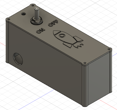
Rocket Launcher Case (Fusion 360)
 

Launcher Hardware Assembly
With the ESP code allowing the desired launch operation, the circuit board, wiring and battery were assembled and added to the 3D-printed case.

Rocket Launcher Test Assembly

During the assembly, it was noted that the pluggable circuit board headers, although simple to install and use, were expensive and consumed space. On the subsequent revision of the board, as displayed below, the pluggable headers were replaced with through-hole solder pads that suit a larger gauge wire.

Updated Launcher Board

Additionally, the toggle switch used for controlling the power was salvaged from another project. There are no manufacturer markings on the switch to generate a Bill of Materials. More clearance was added around the toggle switch body to suit other types of toggle switches such as the model shown below.

Standard Toggle Switch

Complete Test Assembly
For a bench test, a lamp was used as the igniter as pictured below. A short video of the operational launcher is exampled in the video.


The next post will feature the updated launcher circuit board and field testing.

Monday, 25 March 2024

PCB Artwork - Coffee Cup Coaster

Introduction 

In a previous blog, the circuit board drafting tool Altium Designer was used to create circuit board (PCB) artwork. In this blog, a coffee cup coaster was created using the same technique.

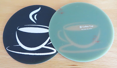
Coffee Cup Holder Front and Back

Removing Colour and Changing the File Format

To begin, select the desired clipart image from your preferred site, such as the image used in this post - a coffee cup. All credit to the original designer and provider of the coffee cup.

Coffee Cup Clipart (Credit Clip Library)

Import the image into an editing tool such as GIMP, Photoshop, or a free online editor. Remove any colour from the image (black and white) to prepare it for use on the PCB. Increase the thickness of the image as needed to ensure ease of production.
After the image editing is complete, save the updated image in a PNG format. This format allows for easy copying and pasting into Altium Designer.

Creating the PCB

To begin creating the PCB artwork for our coffee cup coaster, a circular arc (mechanical layer 1) with an 80 mm diameter to the PCB. This arc defined the board shape and should be larger than the image. An 80 mm diameter suits cups, a 100 mm to 120 mm diameter would suits most mugs.

Coaster PCB Shape and Size

Next, the PNG file contents were copied and pasted into Altium Designer. The imported image is represented by various regions which can be moved as needed.

For the coffee cup, the top copper layer was adjusted using the Properties dialogue box.

Manual Solder Mask Expansion Setting in Altium

To ensure a minimum distance between the solder mask and the copper layer, the solder mask expansion of the copper region was manually reduced to zero using the Properties dialog.

The steam seen above the coffee image was changed to a top-layer silk screen using the same Properties dialog in Altium.

Coffee Cup Coaster in Altium 2D

PCB Export

To prepare the PCB artwork for manufacturing, the file format (Gerber) needs to meet the requirements of the selected PCB supplier. The format may vary depending on the manufacturer and is usually listed on their website. In this post, the JLCPCB supplier was utilised to manufacture the PCB.

Manufacturing

The final appearance and cost of the coaster can vary greatly based on various factors. These factors include the thickness of the circuit board material, surface finish, solder mask and silkscreen colour.
In this post, the board thickness was maintained at 1.6 mm, the surface finish was lead-free HASL (Hot Air Solder Levelled), the solder mask was changed to black on the top side only and the silk screen was kept as white.

Coffee Cup Coaster in Altium 3D

Final Product

Pictured below is an image of the board as supplied by the manufacturer.

Coffee Cup Coaster on the Bench

Due to lighting the contract between the silver surface and the white silkscreen is not captured. To increase the longevity of the coaster, a clear epoxy or a hard-wearing lacquer could be applied. This will prevent the HASL coating from becoming tarnished over time.

Coaster in Use
Coaster in Use

Saturday, 24 February 2024

CTEK MXS 5.0 Pushbutton Switch Replacement

Introduction
This blog follows the process of replacing a faulty mode switch on a CTEK MXS 5.0 battery charger. The symptom of failure was no change in the mode when the mode button was pressed.

CTEK MXS 5.0 Charger
 
Repair Process

With no screws located on the charger case for servicing, YouTube was consulted on methods to open the charger.

For this charger model, the case is a two-part build. The sealing mechanism between the two cases (seam) appeared to be a glue or a plastic weld. The plastic seam was cracked by placing a flat blade (wide) screwdriver on the seam and striking the rear of the screwdriver with a mallet. The break in the plastic was, however, not entirely clean.

CTEK MXS 5.0 Open Case

On separating the case halves, the plastic base of the charger contains what appeared to be some type of isolator.

CTEK MXS 5.0 Case Bottom

CTEK MXS 5.0 Case Lid

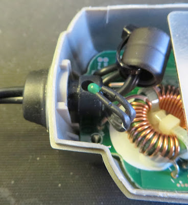
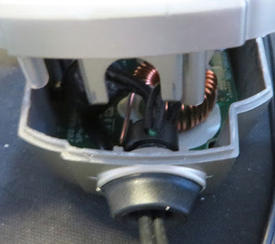
To allow access to the charger circuit board, the cable glands at either end had to be removed. As pictured in the image below, one of the glands has an indent for a thermistor or possibly a thermal fuse.

MXS 5.0 Device in Cable Gland

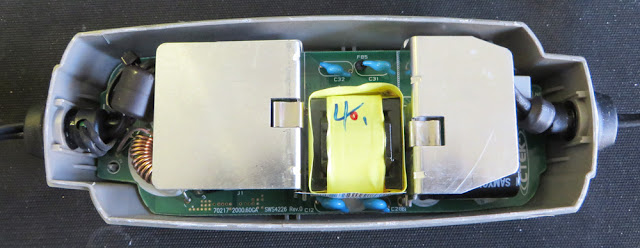
With the board unseated and flipped over, the logic devices, controllers, processor and switch were visible.

CTEK MXS 5.0 Circuit Board

Possibly to prevent damage to the decal, the membrane switch has a plastic cap fitted.

CTEK MXS 5.0 Circuit Board Switch Cap Off

As the pushbutton switch manufacturer and model were unknown, a similar surface mount switch was used. 

For readers preferring to locate an exact pushbutton replacement, the switch body is 6 x 6 mm with a height of 4 mm. The switch plunger height from the switch body is approximately 2.7 mm. The top of the tapered shaft is 3.45 mm. The top of the switch shaft is the side pressed into the button cap.

CTEK MXS 5.0 Factory and Replacement Switch

The plunger height of the replacement switch was manually reduced with a pair of side cutters.

After fitting the replacement switch to the circuit board, the charger was powered and the button operation was tested. The switch cap was then fitted.

CTEK MXS 5.0 with New Switch

Reassembly
The circuit board was moved into position and realigned to fit into the charger's plastic lid.

During the reassembly process, the electronic protection device was reinserted into the cable gland.

CTEK MXS 5.0 Protrusions for Cable Gland

When the two halves of the charger case were pushed together, the two U-shaped plastic protrusions on the plastic base locked the cable glands in position.

Lastly, to permanently join the halves of the charger case, glue was applied to the seams near the cable glands. For readers using the charger in a high moisture or damp environment, fully sealing the seam of the charger is highly recommended.

CTEK MXS 5.0 Charging Battery


Wednesday, 3 January 2024

10Gtek Ethernet to Fibre Converter Teardown

Introduction
This post provides a teardown of the 10Gtek G0101-SFP Ethernet to Fibre Media Converter.

10Gtek Ethernet to Fibre Media Converter

Background
To electrically isolate Ethernet test equipment on the bench, a pair of media converters were being utilised. I wanted to know what was inside the media converters since standalone boards performing the same Ethernet to Fibre conversion were available on AliExpress for less than USD 9.

10Gtek Media Converter Nameplate

Teardown
The case of the 10Gtek converter is of two-part metal construction. Both of the case parts are held together with four screws. At one end of the metal case are two media connections (Ethernet and SFP). Status LEDs are also visible on this side. On the opposite end of the case is the DC power jack.

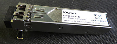
10Gtek SFP  Module
10Gtek SFP  Module

After removing the SFP (Small Form-factor Pluggable) Transceiver and the metal screws for the case, the metal parts slide apart then the printed circuit assembly (PCA) is visible.

10Gtek Ethernet to Fibre Media Converter PCA

The PCA sold by AliExpress look very similar to the PCA used in the 10Gtek unit. On the circuit operation, Ethernet to SFP hardware conversion is performed using a Realtek device part RTL82138.

Elsewhere on the PCA is the metal-cased SFP Transceiver connector, low dropout regulator (ASM 1117 from Monolithic Power Systems), Ethernet magnetics and 25 MHz crystal for the Realtek driver.

It shall be noted that during the disassembly of two 10Gtek units, one of the 10Gtek units contained solder balls on the PCA. Post-manufacturing QA processes commonly identify and remove solder balling.

Solder Balling on PCA

The unit draws approximately 300 mA at DC 5 V when powered. Heatsinking for the regulator was provided using the circuit board. Low Dropout Regulator (LDO) heat generation is a result of regulating the input supply voltage down to 3.3 V.

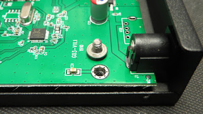
The M3 screws used for retaining the circuit board to the case appear to have oversized heads, or the circuit board footprints are undersized. The screw head's outer dimension measures 6.8 mm however, the circuit board footprint is 5.2 mm.

Mismatch of Sizes for Screws or Board Land Pattern

Additionally, a capacitor is connected between the converters DC 0 V and the case of the unit. If the case is considered Earth, then there is no dedicated external Earth connection provided on the case. The shell of the Ethernet connector is connected to the converter case

Summary
For those seeking just an Ethernet to Fibre converter, many online suppliers have PCAs available. The 10Gtek is useable as manufactured, although a PCA inspection is highly recommended. Also, by applying minor updates to the unit's power supply input, the electrical robustness of the 10Gtek unit could be strengthened.