Saturday, 24 June 2023

Model Rocket Launcher WiFi ESP8266

Introduction
This blog follows the redesign and development of a model rocket launcher controller that features WiFi communications to control the launch process. This design uses an ESP-based microcontroller module. The Arduino platform was chosen for code development.

Rocket Launcher 3D Model

Redesign
To control the launch in the previous model rocket launcher design, Bluetooth communications were used between a PSoC microcontroller and an Android phone. The interface was changed to WiFi to remove the need for developing a phone application. Controlling a rocket launch through WiFi would be independent of a phone or computer operating system.

WiFi Module
For the launcher redesign, an off-the-shelf ESP module capable of WiFi was chosen from Adafruit. The ESP module was chosen for a few reasons. Firstly, the module’s price was relatively low (USD 10). The module was readily available compared to other dedicated microcontrollers. Lastly, using an ESP module meant that the rocket launcher design could be migrated more easily to other ESP devices.

Adafruit Huzzah ID 2471 (Courtesy Adafruit)

Reused Design
The same section of circuit responsible for driving the rocket engine igniter was taken from the previous design. This section consisted of high (VN7040) and low-side (VNL5030) switching drivers (ST Microelectronics).
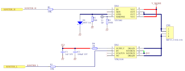
Rocket Launcher Igniter Drive Circuit

Circuit Updates
To begin the schematic update process, the ESP module was created in the schematic libraries. The new part replaced the previous PSoC microcontroller and associated circuitry.

The Altium PCB model was downloaded from the website SnapEDA.

Capture of Adafruit Huzzah PCB Footprint from SnapEDA

Schematic Updates
On the ESP module schematic page, the power supply connections and ST driver control signals were mapped to the ESP.

Rocket Launcher - Huzzah Circuit Connections

Audible notification of an impending launch was retained using the buzzer. Connections were mapped to the ESP.

Rocket Launcher - Buzzer


The display (LCD) was infrequently used in the previous design so it was removed and replaced with an LED.

The launch button input to the ESP module was retained for testing purposes.
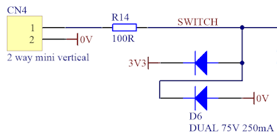
Rocket Launcher - Optional Launch Button

Connections were made to ESP module pins that had no special functions.
 
Output Drivers

Schematic changes were made to the ST output driver’s power supply. This was required to match the ESP module’s DC 3.3 V supply voltage. The feedback monitoring from the ST drivers was removed from the design because of the reliable performance of the ST drivers.

Power Supply
A DC-DC step-down converter was retained for the power supply. Texas Instruments part LMR50410 featuring an integrated diode was selected to replace the previous DC-DC converter.

Another benefit of the DC-DC converter is its operating voltage which is wider than the ESP modules linear regulator (LDO). The LDO has a maximum rated input voltage of DC 6 V. This voltage does not suit all battery chemistry types.

Rocket Launcher - Power Supply

Battery voltage monitoring using the ADC on the ESP through a resistor divider was kept for experimentation and possible future use.

Circuit Board
There were no caveats defined for the shape of the circuit board (PCB). The placement of components drove the PCB shape. Minimal design constraints for the PCB meant that the PCB was set up for components on both sides.

The capture below shows the PCB top layer with the ESP module, power supply underneath the ESP module, buzzer and optional screw terminals. To fit the power supply beneath the ESP module, pluggable headers were utilised to space the ESP module off the board.
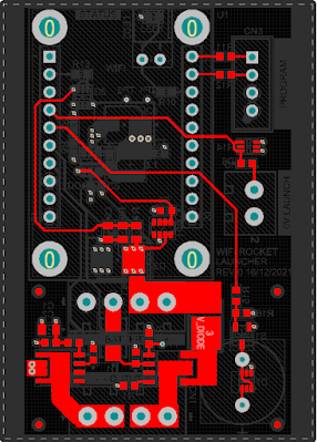
Rocket Launcher PCB - Top Layer

The next capture below shows the PCB bottom layer containing the output switching drivers and related components.
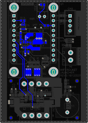
Rocket Launcher PCB - Bottom Layer

Four PCB layers were used for the launcher board stack-up. Captures of the two internal power planes have not been shown.

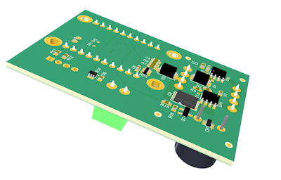
After component placement and routing, the board size reached a comfortable size of 62 x 44 mm. On the longest PCB axis, a set of 3 mm strips were added to suit mounting in an enclosure. Pictured below is a 3D side and rear view of the board.
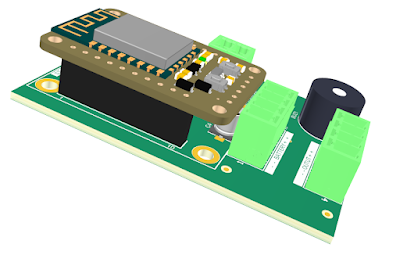
Rocket Launcher - 3D Side View
Rocket Launcher - 3D Rear View

In part 2 of the launcher blog, the PCB construction and initial testing will be performed.

Wednesday, 31 May 2023

Circuit Board Return Path Via Placement Options

Introduction
This blog discusses a few options that new circuit board designers may use for return path vias as a result of signal traces changing circuit board layers through using vias.
 
Further Literature

It is highly recommended that existing content from industry figures such as Eric Bogatin or Rick Hartley are reviewed. Related circuit board information is available from YouTuber channels such as Robert Feranec or Phils Lab to mention a few.

PCB Routing Example
For circuit board designs that feature microcontrollers, microprocessors, FPGA or similar devices with high pin count or spacing density the existing connections to power rails through vias can serve as return paths. In the image below, taken from the Altium Mini-PC board, the green highlighted vias indicate the several 0V (GND) power connections that may function as return paths for the DDR memory address, data, clock and control signals.

Altium Mini-PC Board Highlighted GND (0V) Vias (Courtesy Altium)
 
Reducing Return Path Distance
The capture below is a further extract from the Mini-PC demonstration board showing a distance measurement between a return via and a differential DDR clock pair.

A Texas Instruments Application Note, High-Speed Interface Layout Guidelines, 2023 states that the signal to return via distance should be a maximum distance of 5 mm (200 mil) although that value could be considered design dependent. For the Mini-PC demonstration board, the distance between the return via and differential pair is small, some 2.1 mm.

Altium Mini-PC Board Differential Via Pair (Courtesy Altium)

Consider a situation where the return path distances needed to be reduced. On the Mini-PC board, a smaller distance could be achieved following a circuit board review. Traces on the layers could be moved to make room for a via closer to the differential via pair. The capture below shows one possible change with a reduction to 1.4 mm.

Altium Mini-PC Board with Closer Return Path Via (Courtesy Altium)

Board Space Limitations
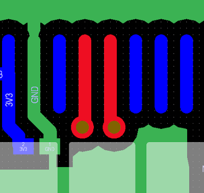
A more common limitation when adding or altering return path vias could be related to circuit board space. In the example below, the traces in the red colour identify a differential pair. There is no return path via in close proximity. The while highlighted rectangles represent pads on the other side of the circuit board.

Differential Pair with No Return Path Via on a Double Sided Circuit Board

The reason for no return path via in the area is two-fold. On the opposite side of the circuit board is a surface mount component with large pads making return via placement difficult. The second limitation is due to the PCB rules. The smallest via hole size is configured for 0.3 mm.

The limitation created by the component on the opposite side can be overcome using a number of solutions. Using the existing circuit board via the size of 0.3/0.5 mm (via hole size/via diameter) three vias could be placed onto the circuit board as shown below. This solution yields a differential pair to return path via distance of 2.3 mm.

Differential Pair with Three Return Path Vias on a Double Sided Circuit Board

Differential Pair with Three Return Path Vias on Other Side of Circuit Board

Another solution to consider is changing the board design rules. The circuit board clearance rule could be reduced from 0.2 mm to 0.15 mm since the smaller clearance is supported by many fabrication houses. 

Paired with the board clearance change, the via hole size could be reduced. For instance, a via of hole size and diameter 0.254/0.444 mm could be selected. In regards to capabilities, circuit board fabrication houses can manufacture smaller via hole/diameter measurement of 0.15/0.28 mm (drilled). Applying the two changes mentioned in this section, a via can then be placed less than 1 mm from the differential pair.

Differential Pair with Single Smaller Return Path Via on a Double Sided Circuit Board

No Space or Other Limitations
For some board designs, it may be impractical to place a via close to a signal that requires a return path. Should board space and routing permit, via stitching throughout the board or a via shielding around the board or relevant section of the circuit may be alternative solutions.

Example of Via Stitching on a Circuit Board

Example of Via Shielding on a Circuit Board

Summary
Even though the placement of return path vias may be a semi-automated process with some software design tools, the lack of circuit board space to position vias in optimum locations still vexes novice and experienced board designers alike. This blog puts that other solutions may be found by reviewing the nominated fabrication house’s manufacturing capabilities and the minimum manufacturing circuit board requirements.

Sunday, 30 April 2023

Salvaging from LG Controller Board EBR369328

Introduction
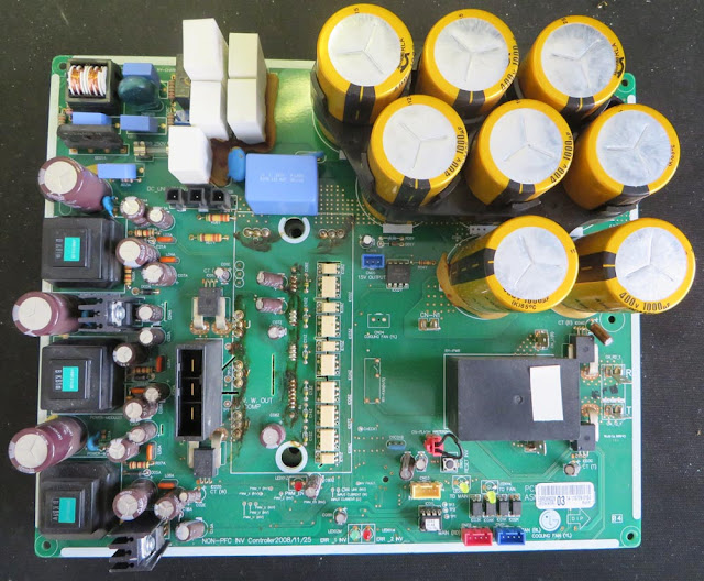
This microblog reviews the electronic components (parts) that could be salvaged from an LG air conditioner compressor inverter controller board.


LG Control Board EBR369328 Top Side

Summary
After being provided with the inverter controller board for spare parts, it seems relevant to detail salvageable electronic components in this blog.

Being unfamiliar with air conditioning (AC) equipment, AliExpress was used to identify the function which is listed as an LG three-phase inverter compressor (motor) control board.

It should be noted that the LG control board was supplied not working. In these instances when salvaging electronic parts, additional
testing and diligence should be taken.

Salvageable Top Side Components
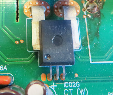
For the current measurement on the three-phase supply, an Allegro device capable of + 50 A, part number ACS756 was utilised. The Allegro part is listed as obsolete however this does not prevent is being used again for testing a
design concept. This is one of the devices that should be tested once removed because of its use in the circuit.

Allegro ACS756
Allegro ACS756

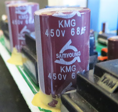
The bulk of the electrolytic capacitors are manufactured by the Korean company, Samyoung. Some of the electrolytic through-hole capacitors associated with the mains (line) supply may be handy for spares if mains voltage projects are an area of interest.

Mains Rated Electrolytic Capacitor

The large 10 to 20 W wire-wound ceramic resistors had no signs of overheating or physical damage. These resistors may be worth salvaging even for simple dummy loads.

Wirewound Resistors
Wirewound Resistors

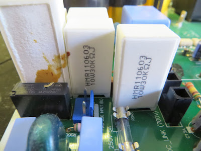
Located near the wire-wound resistors are mains capacitors manufactured by the Korean company, Pilkor. On this LG board, those capacitors were in excellent condition and worth salvaging.

Mains Capacitors
Mains Capacitors

The large vertical connector, AMP series D-5200, should be considered for anyone involved with high-current designs.

AMP Connector D-5200

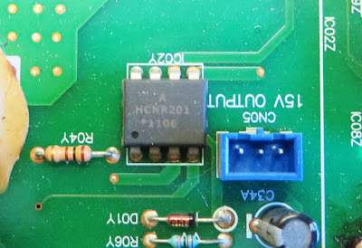
The circuit board is fitted are a few different types of optocouplers. One of the interesting parts is the HCNR201 which is a high-linearity optocoupler from Broadcom.

Broadcom HCNR201
Broadcom HCNR201

Other optocouplers include Toshiba TLP781, TLP559 and TLP521. All these Toshiba optocouplers are obsolete however they may serve well as spares or for repair purposes.

Various Toshiba Optocouplers

A TE relay with the part number T92S7D12-12 is fitted to the board. This relay is rated at a 12 V at 20 A and is still actively manufactured by TE.

High Current TE Relay

Contained on the board are a plethora of remaining components to consider for salvage. These include an oscillator, heatsinks, LEDs, chokes, axial resistors and unidentified components.

Salvageable Bottom Side Components
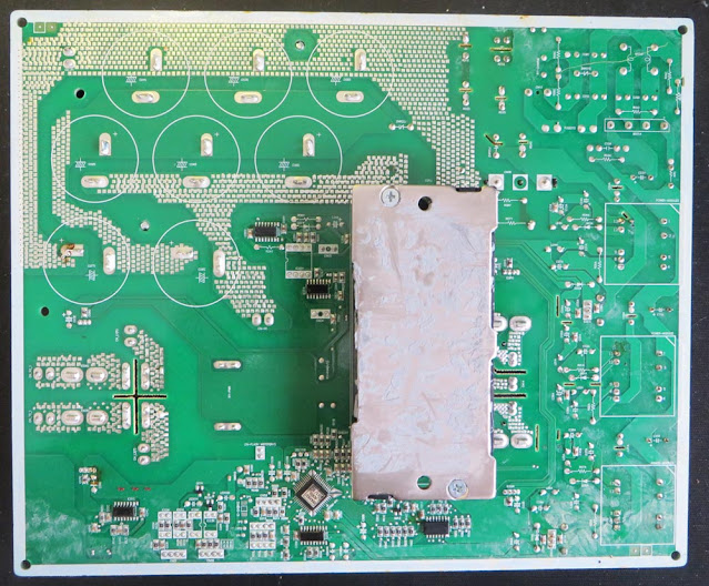
Fitted on the bottom side of the PCB is the motor switching module (IGBT). This device is most likely not worth salvaging.

Motor Driver Module
Motor Driver Module

The semiconductors on the bottom side appear to have no identification markings or those markings have become obscured by what appears to be a protective (conformal or lacquer) coating.

LG Control Board EBR369328 Bottom Side

All electronic parts on the bottom side of the board are epoxy glued to the as part of the circuit board assembly process. There is little to salvage from this side of the board because of the glue although removing components is possible with the correct tools. For low-cost and high-throughput printed circuit board assemblies, soldering using wave solder in a single pass has been a common manufacturing method. This LG board employs some solder-thieving designs in the circuit board layout as pictured below.

Component with Solder Thieving Pads

Sunday, 16 April 2023

Voltage Interruption Tester for EN 61000-4-29 Updated

Introduction
This blog continues from a prior post, Voltage Interruption Tester for IEC 61496-1 Part 5. The interruption tester code detailed in that post was updated to suit supply dips or interruptions specifically to meet the standard EN 61000-4-29.

This original project was posted as a novel example of testing for changes in voltage. However, as interest in this project has been increasing specifically for the DC tests listed in the standard EN 61000-4-29, the code was changed to perform these tests only.

Code Changes
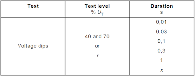
Code changes were implemented in the interruption tester for a closer approximation of EN 61000-4-29 and to improve the code portability between Infineon (Cypress) processors. In the EN 61000-4-29 standard, five tests are listed for DC voltage dips with fixed times of 10 ms to 1 s. An extract from the standard is shown below.

DC Voltage Dip Table from EN 61000-4-29

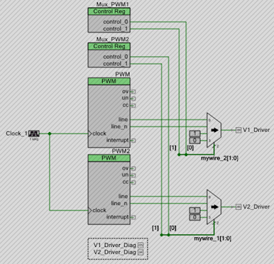
The PWM functionality in the Infineon microcontrollers, configured through the PWM component, was disabled.

Interrupt Tester Project Disabled PWM Logic

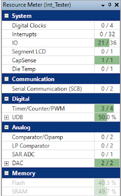
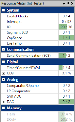
For the reduction in resources controlling the output pins between Cypress PWM and software output control, the Universal Digital Blocks (UDBs) dropped by almost 50 %.

Previous Project PSoC Resource Usage

Updated Project PSoC Resource Usage

The system timer was used as the replacement for the PWM component. Output pins that were PWM controlled are controlled directly in code. To improve the output waveform timing accuracy, the system timer was reconfigured from 10 ms to 1 ms.

Testing Code Changes
Timing control of the outputs controlling the load was performed in the corresponding function listed below.

/** *****************************************************************************
* Function Name: Output_Handler
*
* @brief Run interruption tests with timing below, 10 s separation between tests
*   Test 1 - 10 ms
*   Test 2 - 30 ms
*   Test 3 - 100 ms
*   Test 4 - 300 ms
*   Test 5 - 1000 ms
*
* @return none
****************************************************************************** */
void Output_Handler(uint8_t output_CurMenuItem, uint8_t out_statemachine)
{
    static uint8_t output_savedMenuItem;
    static uint8_t output_driver_state;
    
    if ((out_statemachine == OUTPUT_ON) && (output_CurMenuItem != 0))
    {       
        /* Handle PWM 1 Settings */
        if ((output_driver_state == OUT_OFF) || ((output_driver_state == OUT_LOW) && ( Pulse_Low_Ctr == 0)))
        {
            Pulse_High_Ctr = PWMValues[output_CurMenuItem].COMPARE1;
            Pulse_Low_Ctr = 0;
            output_driver_state = OUT_HIGH;
            V1_Driver_Write(true);
            V2_Driver_Write(true);
        }
        else if ((output_driver_state == OUT_HIGH) && ( Pulse_High_Ctr == 0))
        {
            Pulse_Low_Ctr = PWMValues[output_CurMenuItem].PERIOD1;
            output_driver_state = OUT_LOW;
            V1_Driver_Write(false);
        }
        output_savedMenuItem = output_CurMenuItem;
    }
    else if (out_statemachine != OUTPUT_ON)
    {
        V1_Driver_Write(false);
        V2_Driver_Write(false);
        output_driver_state = OUT_OFF;
    }
}


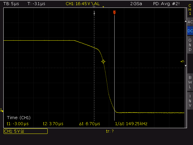
The standard EN 61000-4-29 standard states requirements for the rise and fall times when the tester is driving a 100 R load (
1 us to 50 us).

Test Generator Requirements from EN 61000-4-29

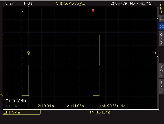
The pulse duration and time between tests were validated with the load.

10 ms Interruption Tester Output
 
100 ms Interruption Tester Output

Testing showed that measured rise times were less than 18 us and the fall time less than 7 us.

Rise Time 10-90 % with 100 R Load

Fall Time 10-90 % with 100 R Load

Future Changes
To facilitate other microcontrollers, another revision of the display circuit board without capacitive sensing, a flat flex inter-board connection, watchdog and adding a third channel to the power board will be investigated.

Downloads
Listed below is the PSoC Creator project.

Interruption Tester 0.1c PSoC Project