Friday, 31 July 2020

Design for Repair Part Two

Summary
This blog continues a previous Design for Repair post with a few further examples which may be applied when designing a Printed Circuit Board (PCB) for repair or serviceability.

Debugging Interfaces
For projects containing devices with firmware or configurable logic such as a microprocessor or FPGA (Field Programmable Gate Array), the capability to debug the design during the design phase is considered necessitous. Customarily programming or debug connections are not available for the end-user or customer, however, this interface can be an effective tool for repair.

Examples of programming interfaces are JTAG, SWD and UART


JTAG 10-Pin. Courtesy Keil
Cypress MiniProg SWD. Courtesy Cypress

Debug Interface PCB Connector
In place of physical connectors such as a pin header, the PCB can incorporate connections using tinned copper or gold fingers when cost saving on components is critical. The image below is an example of a standard UART interface implemented with PCB fingers.


PCB Connector for UART Debug
Surface Mount Component Footprint
Utilising the smallest component footprint in a product's design can, in some instances, lead to the repair of a Printed Circuit Assemblies (PCA) transitioning from an in-house repair process to an external repairer.


SO, TSSOP and DFN Footprints

For the surface-mount packages shown in the capture above, removal of the component could be achieved utilising desoldering tweezers or a hot air rework station. These leaded surface mount components remain the practical choice for a myriad of designs although semiconductor manufacturers are migrating to smaller leadless packages such as UFBGA (Ultra Fine BGA) and DSBGA (Die Sized BGA).

BGA PCB Component
BGA PCB Component

For passive components, footprints such as 0402 and 0603 are a regular package size seen on a PCB design. Smaller package sizes such as 0201 and 01005 normally require additional equipment for board level component repair.

Component Solder Mask
For components with a pad to pad pitch 0.5 mm and smaller, including a solder mask between pads can be a challenging prospect.

The presence of a solder mask 'island' between component pads can be beneficial for service personnel performing rework and during visual inspection. 


PCB Extract Spirit Level U1 Top Layer. Courtesy Altium Ltd

In the capture above the components pad to pad spacing of 0.5 mm was used with the default solder mask expansion of 0.1 mm which resulted in no solder mask between pads.

In the following capture, the default solder mask expansion layer was modified from 0.1 mm to 0.05 mm for the five pads on the right of the image. 

PCB Extract Spirit Level U1 Solder Mask - Modified. Courtesy Altium Ltd

The components pads viewed in 3D below emphasises the change to the solder mask expansion.


PCB Extract Spirit Level U1 in 3D with Solder Mask Modified. Courtesy Altium Ltd

Connector Numbering Using Silk Screen
Numbering connector pins using a PCB overlay removes uncertainty and may well be a labour-saving for service personnel. Consider the capture of the connector below where pin numbering has not been provided on the silkscreen.


PCB Extract Spirit Level with Numbering Removed. Courtesy Altium Ltd

The second capture, shown below with the original silkscreen, conveys the pins numbering legibly. For a densely populated board, free space on the silkscreen may not allow for numbering of individual pins. In these instances, a constant incrementing pin numbering pattern may still be beneficial for service personnel.


PCB Extract Spirit Level with Original Numbering. Courtesy Altium Ltd

Danger or Hazard Identification Using Silkscreen 
A PCB silkscreen can be used to convey functional information relating to the PCB, product operation and any dangers service personnel may be presented with. 


High Voltage Identification Using PCB Silk Screen

In the example design above, the silkscreen on the PCB provides details relating to the relay contact operating voltage.

PCB Test Point, Pad and Via
Adding the function of a test point to a components silkscreen was mentioned in the previous Design for Repair (DFR) post as a benefit for service personnel.

Other aspects of the test point which may need to be considered during PCB design include, fitting of a physical component, test point hole size, test point annular ring size or single-sided compared to a through-hole pad.


Test Point, Via and Pad

In the capture above, PCB mount Test Point TP2 is fitted to the board.

TP18 is the same component as TP2 and is not fitted to the board. With a sizeable diameter of 3.7 mm, this test point may not be suited for boards with a high component or routing density.
 
TP19 is a more common test point size. This features a 0.5 mm hole with a 0.8 mm annular ring. A hole of approximately 0.3 to 0.5 mm, without solder mask tenting, allows reliable connections with an oscilloscope or multimeter probes. Should there be a requirement, wires can be soldered to the thru-hole pad.
 
A major drawback with TP2, TP18 and TP19 is the area used by thru-hole parts which apply to all layers on the PCB.
 
One of the most common test point types shown in the capture is TP20. This test point is provided as a pad on a single side of the PCB. Pad diameters may range from 0.2 to 0.8 mm. Usually, this test point is used for In-Circuit Testing or programming boards. An important detail is the test pad wastes no real-estate under the pad compared to a thru-hole via. Wires can be soldered to the pad however it lacks the robustness of a thru-hole pad.

Surface Mount Nuts, Spacers and Standoffs
Disassembly and assembly of a product may constitute a significant portion of a products repair time if individual nuts, bolts, washers and stand-offs are used. Another option to minimise individual hardware items may be surface mount nuts or spacers.


M3 Self Clinching Nut (PEM)

Companies such as Pemnet, Würth Electronik and Keyelco manufacture hardware suitable for most designs.

SMT Right Angled Surface Mount Block. Courtesy Würth

Final Thoughts
As each product design is unique, the examples in this blog should be drawn from a designers cache when applicable.


Friday, 19 June 2020

Salvaging Parts BiPAC 7800VDOX

Summary
This post details which circuit board components could be salvaged from a Billion BiPAC 7800VDOX Wireless Router.

BiPAC 7800VDOX Wireless Router

Router Disassembly
To separate the Wireless Router's grey lid from its base, four rubber feet located on the base of the router enclosure were removed. The removed feet expose the screws retaining the lid.

BiPAC 7800VDOX Wireless Router PCB

The above image shows the Wireless Router internal Printed Circuit Board (PCB) with the light pipe and rear panel removed.

Parts to Salvage
Cabling
There are two antennas in the lid with RF connectors (RSP / AMC style) which could be salvaged.

Heat Spreaders
On the PCB are several ceramic heat spreaders (heatsinks) attached to various Broadcom components. These are held down with double-sided tape.

Mounted Heat Spreaders

Removing the heat spreaders can be achieved using a tool such as a wide flat blade screwdriver to lever the heat spreaders off carefully.

7800VDOX Wireless Router PCB No Heat Spreaders
7800VDOX Wireless Router PCB with No Heat Spreaders

Removing the heat spreaders exposes the Broadcom chipsets comprising of the processor, RF and communication hardware. The Broadcom hardware is not suitable for salvage, possibly repair to a similar router.

Inductors
There are open core leaded and PCB mount inductors which could be recycled for other designs.

Wireless Router PCB Inductors

Diodes
Identified in the image below are single and dual colour surface-mount LEDs.

Wireless Router PCB LEDs

Oscillators
A 25 MHz thru-hole Crystal is located next to the Broadcom chip responsible for the Ethernet clock and a second surface mount Crystal oscillator can be found by the Broadcom processor.

Wireless Router PCB Oscillators

Relays
The two Fujitsu FTR-C1CA003G miniature relays have a coil operating voltage of 3 V DC with DPDT 1A contacts. These thru-hole relays are worth removing.

Wireless Router PCB Relays
 
Resistors
Distributed across the top and bottom side of the PCB are resistors with case sizes larger than 0805 which can be repurposed. Most are standard resistor values.

Wireless Router PCB Resistors

DC-DC Regulators
A mixture of Fitipower DC-DC Step Down Switch mode chips (FR98860 and FR9888) could be removed.

Wireless Router PCB DC-DC Controllers

Connectors
The vertical USB connector and DC jack could be removed and reused in another design. Removing and reusing the right-angle Ethernet or RJ connectors should be achievable.

Capacitors
Any of the radial Electrolytic capacitors could be reused. It should be noted that the Su'scon capacitors (SD and SK series) although rated with a useful operating temperature of 105°C (max), have a 2000 hour operating life at the maximum rated temperature. Consider that the Wireless Router may have been operating for 10 years continuously which may have significantly reduced the lifetime of the capacitor.

The other surface-mount Electrolytic capacitors (22uF) appear to be the Panasonic FK series which are rated to 105°C with a 2000 hour operating life at the maximum rated temperature.

Wireless Router PCB Capacitors

Unlisted Components
Several additional types of components could be removed from the Wireless Router PCB although some are extremely small (0402 footprints), obsolete or specific to the product. The components listed in this post should have equivalents from different component manufacturers allowing salvaged parts to be used in a prototype PCB design or used for repair.

Monday, 1 June 2020

Mikroe Buck 5 Click with PSoC5 VDAC

Summary
This post examines alternate means for driving the MikroElektronica Buck 5 Click hardware. First, the onboard digital Potentiometer was rewired in a new configuration and second the Potentiometer was replaced with Cypress PSoC.

Buck 5 Click - Courtesy MikroElektronica

Buck 5 Click with Digital Potentiometer and PSoC5
MikroElektronica's Buck 5 Click (MIKROE-3100) hardware presented itself as a cost-effective and off the shelf unit for testing the MAX17506 DC-DC Converter. The Buck 5 Click was designed primarily for use with other MikroElektronica hardware. The input voltage range of the Maxim buck converter (4.5V to 60 V DC) is not fully utilised on the Buck 5 Click (5V to 30 V DC). In the same manner, the output voltage appears capped at 20 V DC maximum. Even with the voltage limits the output range of the hardware was able to be tweaked. 


Wiring a Cypress CY8CKIT-059 prototyping kit to drive the Buck 5 Click required three connections for the SPI and two for power. The Buck 5 Click schematics indicated the board logic operated with 3.3 V DC however, the board was powered from 5 V DC. The supply range of the MAX5401 digital Potentiometer (pot) was 2.7 V to 5.5 V DC.

To control the digital pot, a PSoC Creator application using an SPI Master component was created


SPIM_WriteTxData(Buck5_Dig_Pot_Val);
while (0u == (SPIM_ReadTxStatus() & SPIM_STS_SPI_DONE)) 
{ }


The subsequent step of increasing the output voltage range of the Buck 5 Click was accomplished although the configuration of feedback resistor network (R8) and digital pot (U2) for the DC-DC converter (MAX17506) needed to switch places. The digital pot operating voltage was the reason for the change. The pot wiper was connected directly into the feedback pin of the MAX17506. Below is a working board with modifications.


Buck 5 Click Modified with Increased Output Range


The output voltage range of the modified board was approximately 4V to 18 V DC. The digital pot, with 255 positions, provided output voltage steps of 55 mV.

When applying power to the digital pot, the default setting is the middle position which may not be ideal in all instances. To control the behaviour of the buck regulator on power-up, a connection from the PSoC to the Enable line of the Buck 5 Click was used. A pull-up resistor (R4) was removed from the board to prevent the Buck 5 Click from starting when power was applied

Buck 5 Click with Cypress PSOC5 VADC, No Digital Potentiometer
Other solutions for adjusting the output voltage of a DC-DC converter, through control of the feedback pin, use external PWM or DAC sources.

The Cypress PSoC provides control of DC-DC converters either through PWM (Trim and Margin component) or a DAC (Current or Voltage component). This post used the PSoC VDAC8 component which provided 255 steps. For additional resolution the dithered VDAC component with 4096 steps could be used.

For calculating the output voltage for VDAC solution, Maxim published a notable tutorial deriving the output equation shown below from first principles.

VOUT = VREF(1 + (R1/R2)) + (VREF - VDAC) (R1/R3)                        Eq (1)

For connection of the VDAC to the feedback loop of the DC-DC Converter, one additional resistor (R3) was required.


DC-DC Converter Output Voltage Control Using a DAC

A spreadsheet was used to implement Equation (1) which allowed the three unknown resistor values to be manually changed and the output voltage range of the DC-DC converter observed.

DC-DC Converter Vout Spreadsheet Calculations

Equation (2) was used to ensure that the maximum current seen by the PSoC (DAC) was less than 25 mA.

i3 = (VREF - VDAC)/R3                       Eq. (2)

Quadrature Encoder
A quadrature encoder (Bourns PEC11R) was added to the design to allow for manual voltage adjustments. The QuadDec component was used to convert the encoder AB lines. The QuadDec returned value was limited to between 0 and 255. The reading from the QuadDec was then used to adjust the output of the VDAC component.


PSoC Creator Top Design
The project required the QuadDec, DAC and OpAmp components as shown below.


PSoC Creator Project Top Design


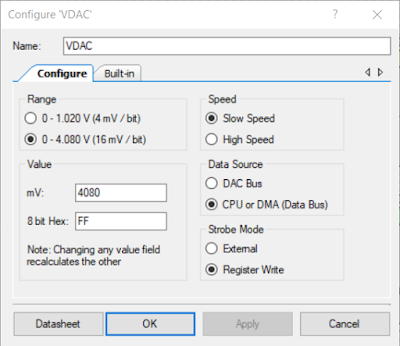
The calculations in Excel used a voltage range from 0.1 V to 4.08 V which was the option selected in the VDAC component.

VDAC Component Settings

While not essential, an OpAmp follower was added to the design.

OpAmp Component Settings

To maintain 255 positions the QuadDec component was changed from the default 8 bit to 16 bits.

QuadDec Component Settings

The remaining signals that are shown on the PSoC Creator project page (Top Design) were related to the DC-DC converter (PSU_Enable) and the on-board switch (Switch1). Voltage ramps were generated in code on start-up then Switch1 was pressed.

To facilitate testing of the encoder, a UART component was added to the project.

PSoC Creator Pin Mapping
Pin mapping for the design is shown below.


PSoC Project Pin Mapping


PSoC Creator Code
Listed below is an extract of some quick and grubby code used for testing the Mikroe with the PSoC Creator prototyping board.


/**
* @brief Main init and update VDAC based on quadrature encoder value
*/
int main()
{
  uint16_6 Encoder_Count, Encoder_Count_last = 0;
CyGlobalIntEnable();
QuadDec_Start();
UART_Start();
Opamp_Start();
VDAC_Start();
CyDelay(2000); /* Time to stabalise */
PSU_Enable_Write(true); /* Switch DC DC On */
pulse_on_switch1();
for(;;)
{
Encoder_Count = QuadDec_GetCounter();
if (Encoder_Count != Encoder_Count_Last)
{
if ((Encoder_Count <= MAX_ENC) && (Encoder_Count >= MIN_ENC))
{
write_to_uart(Encoder_Count);
VDAC_SetValue(Encoder_Count);
}
else if (Encoder_Count > MAX_ENC)
{
Encoder_Count = MAX_ENC;
QuadDec_SetCounter(MAX_ENC);
}
else if (Encoder_Count < MIN_ENC)
{
Encoder_Count = MIN_ENC;
QuadDec_SetCounter(MIN_ENC);
}
Encoder_Count_Last = Encoder_Count;
}
}
}

The functionality of the test code was to read the Quadrature Decoder, ensures the value read was within the range, then write the value to the VDAC.


Hardware Setup
Shown in the image below is the hardware setup which consisted of the Buck 5 Click, PSoC board and the rotary encoder.


Buck 5 Click with Increased Output and PSoC VDAC

Output Voltage Range and Regulation
The calculated output voltage range was for 1.62 V to 20.33 V DC and the measured range was 2.39 V to 20.42 V DC.

Rudimentary load tests were conducted with a resistive load driven by the Buck 5 Click. Tests indicated a 0.25 % voltage regulation with low loads (1W) and better than 0.1 % with higher loads (65 W). The DC-DC converter used in the Buck 5 Click (MAX17506) has a capability of 5 A. The full load current was not load tested.

Output Voltage Adjustment using PSoC
To change the output voltage of the DC-DC converter without the encoder, the value written to the VDAC was controlled in software. When the switch located on the Cypress CY8CKIT-059 prototyping kit was pressed on power-up, the code generated several pulse types.

Buck 5 Click Output Voltage Waveform from PSoC VDAC
Buck 5 Click Output Voltage Waveform driven from PSoC VDAC

The capture above shows the Buck 5 Click output voltage ramp up and down with a 220 R resistive load.

Final Thoughts
The MikroElektronica Buck 5 Click was a reliable hardware module which allowed a Cypress PSoC to be interfaced for testing. Using a DAC to adjust the output voltage provided an alternative method to the on-board Potentiometer. The option to use PWM control for voltage adjustment was not reviewed in this post although this method should be considered as another solution.


Downloads
PSoC Creator 4.3 Power Supply Project (PSU) Project.

PSoC Creator 4.3 PSU Project

Saturday, 2 May 2020

PSOC Unused I/O Pins

Summary
This blog reviews GPIO configurations for unused PSoC microcontroller pins with a focus on the resulting differences in current usage.

Cypress PSoC4 Controller

Existing Literature
Information relating to the handling of unused pins can be located for most microcontrollers, for example AVR or Microchip. Companies such as Analogue Devices have posted similar unused pin information in their monthly Analog Dialogue.

Between the Cypress Technical Reference Manuals (TRM) and the Cypress community forummethods for handling unused processor pins have been detailed or discussed in numerous times.  Forum suggestions for managing unused pins varies from configuring the pins as high impedance digital inputs, to resistive pull-up/pull-down to outputs.

The PSoC4 TRM states on page 64 under the High Impedance Analogue heading that unused GPIO pins should be configured as high impedance analogue pins (PSoC 4100/4200 Family PSoC 4 Architecture TRM, Document Number: 001-85634 Rev. *H).

While the TRM does not detail the benefits of terminating unused pins with pull-up / pull-down resistors or the effects of EMC / EMI on floating pins, one of the salient remarks in the extract from the TRM is 'unused GPIOs must be configured to the high-impedance analog'. The previous comment relates primarily to current consumption in low-power modes, however the pin configuration could be inferred for unused pins.

High-Impedance Analog
High-impedance analog mode is the default reset state; both output driver and digital input buffer are turned off. This state prevents an external voltage from causing a current to flow into the digital input buffer. This drive mode is recommended for pins that are floating or that support an analog voltage. High-impedance analog pins cannot be used for digital inputs. Read-ing the pin state register returns a 0x00 regardless of the data register value. To achieve the lowest device current in low-power modes, unused GPIOs must be configured to the high-impedance analog mode.

For pins configured as high impedance (digital), Electronic Design is one of the sites which details the reason why high impedance digital inputs are not preferred. An extract from the Electronic Design site is detailed below.

Over time, however, the floating input tends to accumulate a charge and float toward the logic level change-over point. When it reaches that point, it causes both the high and low MOSFETs to be partially on, resulting in shoot through current.

To provide a visual representation of shoot through current mentioned in the above extract, consider a post such as this from the Texas Instrument forum.


Shoot Through Current - Courtesy Texas Instruments

Certainly other technical sources indicate that pin configurations should be resistively biased or configured as outputs only. Time to perform a few measurements to verify the pin configurations!

PSoC Current Measurements 
To perform current measurements of the PSoC4 on the bench, a surplus PCB from a previous project was loaded with minimal components. A PSoC4, a pull-up resistor for the reset line and some essential capacitors were fitted to the board.


Cypress Microcontroller with Unused Pins

PSoC Programming was performed using a Miniprog.

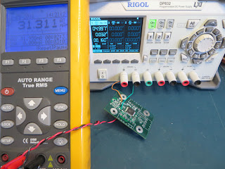
The supply (5 VDC) was provided from a bench supply, Rigol DP832, as shown in the image below. Current measurement was made using a standard digital multimeter.

PSoC4 Bench Setup for Current Measurement

The PSoC Creator application used the pin component to configured the entire port. Any change made to the pin type was reflected for all pins on the port.

PSoC Creator Top Design All Pin Configuration

Two current measurements were taken as verification. The power supply current measurement was verified against the multimeter.

Measurement Results
Measurements were performed on a PSoC4 (CY8C4245AXI-483) with GPIO drive modes (type) 0 - 4 and 6 - 7.


PSoC4 GPIO Drives Modes
PSoC4 GPIO Drives Modes - Courtesy Cypress Semiconductor

For the GPIO types listed in the table below, the default PSoC Creator settings were used. All pins were configured for contiguous mapping except for high impedance analogue inputs which required the contiguous mapping to be disabled.

PSoC4 Overall Current Measurement for GPIO  Configurations
PSoC4 Overall Current Measurement for GPIO  Configurations

The High Impedance Digital Input GPIO type had a striking difference in measured current compared to the other types.

Final Thoughts 
High Impedance Digital Inputs resulted in the highest overall current consumption of an active PSoC4 device. From the brief range of measurements performed in this post it would be prudent not to configure unused PSoC pins as High Impedance Digital.

Unused PSoC pins should be configured with internal resistor biasing or as outputs where practicable.

PSoC Project
For readers interested in verifying or disprove this post, the PSoC Creator project is made available.


PSoC Creator Project - Test PSoC