Saturday, 23 April 2022

Voltage Interruption Tester for IEC 61496-1 Part 2

Summary
This blog follows a previous post where the concept for a supply voltage interruption tester (unit) was validated.

In this blog, the design was formalised by implementing the design on circuit boards using available electronic components. The alternate design supports operating voltages from DC 8 V to 60 V at 2.5 A.
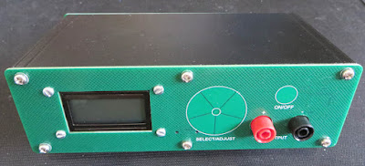
Voltage Interruption Tester Prototype

The design goal was to create a cost-effective unit that would provide indicative testing for Section 4.3.2.2 Supply Voltage Interruptions of the standard IEC 61496-1. The testing is indicative because this units is not an IEC qualified unit.

Two external power supplies supply the voltages that are switched by the unit to generate the required output waveforms.

In addition to the standard IEC tests, two additional tests were added; one for generating repetitive mains frequency noise (50 Hz) and the second for testing diodes such as Transient (TVS).

Example Output Waveform from Voltage Interruption Tester

Editing the project source could yield additional or completely new tests.

Hardware Overview
Three circuit boards (PCB) were created. These consisted of a front, rear and internal PCB. For ease of use on the bench, the design was made to suit a small aluminium enclosure. The two boards containing electronic devices detailed below.

Power PCB Prototype
Power PCB Prototype (Top Side)

The first board, labelled the power board, contained a DC 3.3V regulator with an operating range of DC 4 to 60 V, high side drivers, pluggable power banana connectors and an optional USB interface. The high side driver operating voltage is DC 8 to 60V.

Power PCB Prototype
Power PCB Prototype (Bottom Side)

The front PCB was also purposed as the unit's panel. This board contained a Cypress microcontroller and a two-line LCD.

Display PCB Prototype
Display PCB Prototype (Bottom Side)

Buttons were implemented on the PCB using the Cypress Capsense interface.

Display PCB Prototype
Display PCB Prototype (Top Side)


Power PCB
The power PCB was created as a double-sided board so that the two high side switches (IPS160H) could take advantage of heat dissipation to the aluminium case if needed. Signals from the high-side switches were provided to the microcontroller although monitoring was not implemented at this time.

PCB mount banana plugs provided the connections for the dual supply inputs and voltage interruption tester output.

Powering of the microcontroller and LCD on the display PCB was realised using a DC 3.3 V wide operating range DC-DC switchmode (LMR16006XD). The switchmode will begin operating with an input voltage of 3.6 V which may be useful for high side switches with a lower operating voltage.

Debug and diagnostic feedback were provided through an optional USB interface.

A resistor population option allows for the selection of the switchmode supply source. This could either be input voltage 1, 2 or the optional USB.

Display PCB
Contained on the display PCB were the microcontroller and two-line LCD.

Prototype Supply Interruption Tester LCD

An interface for the operator was achieved using PSoC Capsense buttons. Capsense signals were interfaced to the Cypress microcontroller providing a five-element radial slider and an On/Off button. The cross-hatching pattern seen on the PCB significantly helps with the Capsense operation.

Rear PCB
There were no components mounted on the rear PCB however the front and rear PCBs used the silkscreen to provide the relevant operational information.
 
Rear PCB Prototype
Rear PCB Prototype
 
 
Continued in Part 3

Tuesday, 15 March 2022

Tray Insert for Altronics H0235/H0236

Summary
This brief blog shows how a 3D printer can be used to extend the life of unused equipment. In this blog, the item reviewed was plastic parts drawers.


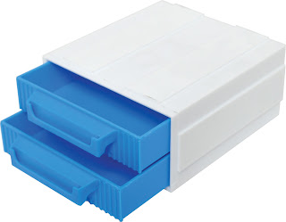
Plastic Parts Drawers Courtesy Altronics Distributors

Repurposing Drawers
After mothballing several stackable plastic part drawers because they were not suited to hold electronics parts, it was decided to reuse the drawers.

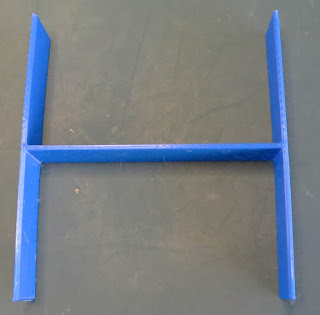
To repurpose the drawers, the internal storage area was halved to hold fasteners and spacers using an insert. This was achieved by creating a suitable model in a CAD package.

3D Printed Draw Insert
 

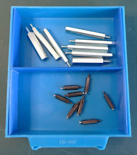
The image below shows how the draw storage area was fitted with the plastic divider insert. The end result was that ten plastic drawers split into twenty storage spaces.

Plastic Drawers with Insert

Downloads
The plastic diver insert was created in Fusion 360, converted in Cura and verified by printing on an Ender 3 printer.

The CAD file could be modified to suit the single part drawer, sold as H0235 by Altronics.

Draw Insert Fusion 360


Draw Insert STL

Thursday, 10 March 2022

Salvaged PCB Reuse with CMS12530

Summary
This blog describes how salvaged electronic hardware, such as circuit boards, can be repurposed for alternative tasks.

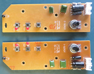
Salvaged Circuit Boards from Kitchen Appliance

Overview
The board (PCB) described in the blog was removed from a kitchen appliance (toaster) when repairing the appliance was not possible. When a requirement came for a basic timer, rather than scrounging for a 555 timer to place on Veroboard or trawling the web to purchase a microcontroller to use as a timer, the toaster PCB was recalled. Time to play!


PCB Description
Used on the PCB was an integrated circuit (IC) from CMSemicon (China), part CMS12530. The CMS device represents the brain of the operation, performing timing and output control. The additional pushbuttons define the operations and the potentiometer to vary the timers operating time.

Salvaged PCB Solder Side

Since the PCB was a simple design, it was decided to transpose the circuit into Altium Designer, as pictured below.

CMS12530 Circuit from Salvaged Appliance

The operating voltage of the PCB hardware was not determined during the salvage operation, so a low input voltage was selected for testing.


PCB Testing
A bench power supply providing DC 12 V was connected to the connector IN.  After powering the PCB, pressing the Defrost or Reheat buttons resulted in the corresponding LED switching ON however the LED did not switch OFF.

No wiring had been made to the PCB OUT connector. It was determined that the output transistor Q1 was normally ON after power-up, then switched OFF after the timer had expired.

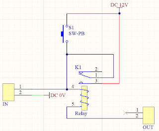
The push to activate function of the toaster needed to be simulated. To achieve this function, a latching relay utilising a single contact was added to the circuit.

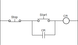
Start-Stop Control Courtesy Accautomation

With the addition of a push-button (Start), the relay could be latched. The stop operation was resolved using the output transistor.

Circuit to Power Salvaged Appliance PCB
 

When the start button S1 was pressed the relay latched and the CMS controller began timing. If no buttons on the PCB were pressed, the timing operation was normal. Otherwise, the Defrost, Reheat or Stop button operation took precedence.

Connections to Salvaged Appliance PCB

After the timing cycle was completed by the controller, the transistor Q1 unlatched the relay thereby disengaging power to the PCB. Reactivation of the timer required the Start button to be pressed again.

Summary
The reverse engineering and initial testing in this blog were sufficient to verify that the salvaged PCB could be repurposed as a basic timer. The PCB in this blog would not be recommended for commercial or industrial purposes, however until the supply of global electronics return to a stable level, the use of salvaged electronic hardware may provide value for specific solutions.

Sunday, 20 February 2022

Example Lids as Circuit Boards (PCB) Part 2

Summary
This short blog
follows on from the previous blog listing some drawings for lids/plates that were replaced with circuit boards.

Hammond 1455N1601 with Press Fit Panel

Circuit Boards Lids
While the previous blog used a clearance of at least 0.1 mm per edge, some of the new lids used an interference fit. Board dimensions should be validated to suit each design.

Again for verification, the Altium Designer files were saved as STEP files, converted to STL files then 3D printed before manufactured.

The DXF files below were generated using the Export feature in Altium Designer. The listed DXF files can be imported into an Altium PCB project using measurements in millimetres.

PCB Lid DXF for NUB505017

Saturday, 15 January 2022

PSU Repair JT-DC12C5A

Summary
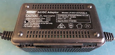
This blog details the repair of a JT-DC12C5A(II)-A switch-mode power supply.

JT-DC12C5A Power Supply
 
Details
The switch mode power supply displayed above had been operating under high load for an extended period before failure. After failure, the DC 12 V output had reduced to less than DC 2 V.

Disassembly
Note: For repair to any AC 240 V equipment, due care and attention should be taken before undertaking service work or repairs. Unplug equipment before performing repairs!

Four plastic clips are integrated into the housing and one plastic screw hold the two-piece enclosure together.

After prying the case apart, the power supply circuit board was attached to the enclosure base plate.

JT-DC12C5A Circuit Board

Servicing
A quick visual inspection of the board did not identify any burnt or charred sections on the PCB. The mains fuse continuity was good.

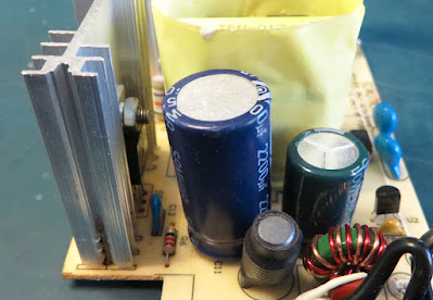
A slight bulge was noticed in one of the electrolytic capacitors located on the DC output stage. As shown in the image below, the top portion of the leftmost electrolytic capacitor is bowed upwards.

JT-DC12C5A Bulged Capacitor

The suspect capacitor was unsoldered from the power supply PCB and checked with a capacitance meter. The measured capacitance was 1 nF where the capacity listed on the case was 470 uF.

JT-DC12C5A Replaced Capacitor

A capacitor with a larger capacity of 2200 uF and the same working voltage was fitted to the circuit board.

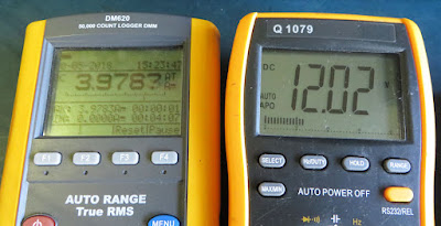
The unit was powered and a 2 A load was fitted to the output. Measuring the output voltage with the load was approximately DC 12.1 V.

JT-DC12C5A Output Load Test Measurements

The unit was reassembled and another load test was conducted at around 4 A. Operation was verified by measuring the output voltage, approximately DC 12 V.

Summary
As far as power supply circuit boards repairs rate, this was uncomplicated. However, the change to the output capacitor was made to address possible ripple currents in the output that may have damaged the smaller capacitor. As always, the component specifications should be verified before replacing in any repair.

Friday, 7 January 2022

Electronic Component Reel Clip

Summary
This blog provides a solution to tidy partially consumed electronic component reel/spool tape using a 3D-printed clip.

Clip for Electronic Component Reel

On-Reel Clip
For infrequently used component reels, an on-reel clip can be attached as shown above to secure the tape. The 3D-printed clip features a slot through the clip body for securing the tape. This prevents the unnecessary unwinding of a reel when stored.

Loose Component Reels

Reel Types
Component reels come in various diameters and packaging which can result in different spool characteristics. The clip dimensions were adjusted to suit different for suppliers such as Multicomp Pro, Philips, Yageo, Vishay, Wurth and likely more manufacturers.

For this blog, two reel types were used. The more common reel uses a thin or narrow reel frame and others had a thicker frame. Narrow clips use a 1.2 mm gap and Wide use a 1.9 mm gap to clip over the reels as illustrated below.

Closeup of Fitted Clip

Reel Clips
To assist in identifying the type of components on a reel, the first letter of the component was embossed on the outside face of the clip. R for resistor, C for a capacitor and a generic N for no marking.

The printed clips used a 0.16 mm printer resolution, material was PLA+, no raft and no supports.

3D Model of Component Clip

Downloads

These files are free for personal use.
Reel Clip - Narrow - None

Reel Clip - Narrow - Capacitor
Reel Clip - Narrow - Resistor
 
Reel Clip - Wide - None
 
Reel Clip - Wide - Capacitor
 
Reel Clip - Wide - Resistor


Monday, 27 December 2021

Salvaging Motorola MBP11

Summary
This blog performs a teardown of the Motorola MBP11 baby monitor, comprised of a transmitter and receiver unit, for the purpose of salvaging electronics.

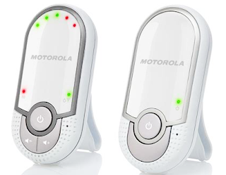
Original Image Motorola MBP11
Original Image Motorola MBP11 (Rights reserved)

Dismantling
The receiver unit of the MBP11 was commonly battery powered by a small NiMH battery. Removing the battery cover allowed access to two plastic screws holding the two-part case together. Whilst the battery could be salvaged, the battery chemistry and capacity may limit use.
For the MBP11 transmitter unit, the two plastic screws holding the case together were accessible from the rear of the unit.
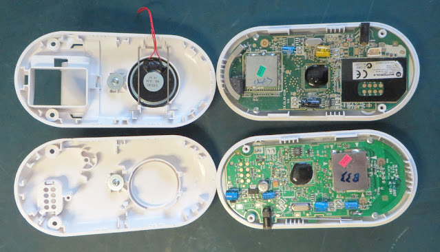
Removing one side of the plastic housing provided access to the circuit boards as shown below.

Opened Cases of Motorola MBP11 Units

Receiver Unit
Holding the receiver circuit board in position were additional plastic screws. The speaker connections were disconnected when the half plastic cases were brought apart.

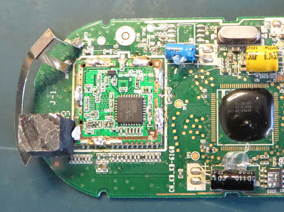
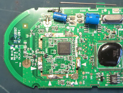
Located on the circuit board were only a handful of salvageable items. The processor was the usual ‘blob’ solution and the RF was all handled in a metal can fitted to a castellated daughter board.

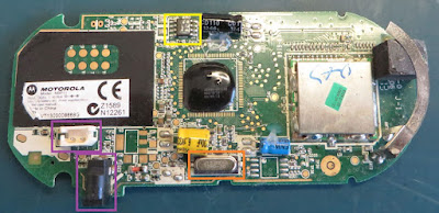
The orange box in the image below shows the 13.842 MHz surface mount crystal used by the unit.

Identified in the yellow box, a serial memory device. The FRAM serial memory part FM24C16B would be worth salvaging especially due to the long data retention of FRAM.

Motorola MBP11 Receiver Circuit Board

Connectors shown by the purple box may come in handy if the battery or external DC 6 V plug pack were used for another purpose.

Out of curiosity the metal can on the castellated RF board was removed.

Under the RF Can on the MBP11 Receiver Circuit Board

Under the metal can was an RF chip, DE 19RF 19CNC, from a chip manufacturer called DSP Group. No immediate datasheet could be located for the chip.

Although the RF chip may not be worth salvaging, the implementation behind the castellated daughterboard is a good example of what can be achieved especially with RF.

There are a few takeaways for new circuit board designers attempting castellated boards including items such as the castellated pad spacing, RF shielding and component placement. As an example, shown by the red box in the image below, the power rail (one side) was decoupled on the main circuit board immediately after the via, then at the RF chip itself.

Decoupled Power Highlighted for Receiver Castellated Circuit Board

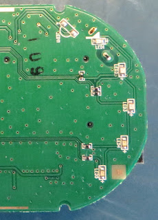
There were seven LED's on the rear of the circuit board that could also be salvaged. Five LED's provided visual feedback for the sound level detected and the remaining indicating connectivity and power. Worth salvaging just for prototype boards.

LED's on MBP11 Receiver Circuit Board

Transmitter Unit
Similar to the receiver unit, the transmitter circuit board was held in position were two additional plastic screws.

The same ‘blob’ solution and RF in a metal can was present on the transmitter board with no castellated circuit board.

The orange box showed the same 13.842 MHz surface mount crystal as the receiver and the yellow box shows the same FRAM device.

Identified by the purple box was the power connector jack.

Motorola MBP11 Transmitter Circuit Board

Highlighted by the black box, the solitary surface mount capacitor. Manufacturer unknown.

Additionally, a linear regulator was present on the transmitter. The red box shows the LM1117. This device could be salvaged also.

The metal can was removed to show the same RF chip as the receiver unit, DE 19RF 19CNC.

Under the RF Can on the MBP11 Transmitter Circuit Board

For both boards, the leaded electrolytic capacitors showed no signs of wear and could be salvaged if needed. All manufacturers of these electrolytic capacitors are not well known. However, some devices are rated to 105°C. Similarly, there are dozens of passive components on the board that could be pried off if required.

Additional Salvaged Items
 

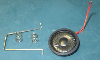
There were additional items such as the PCB mount microphone, external speaker, metal clip and springs that could come in useful for a variety of jobs.

Final Thoughts
There were further items to keep in mind regarding the technology used by these circuit boards such as the gratuitous use of test points, the practical use of via stitching in the RF area and associated power traces.

One item of caution however was the lack of Lead-Free marking on the circuit boards. For the intended target market of the Motorola MBP11, Lead-free would be no less than expected. However, as Lead-free was not noted on the circuit boards, for those salvaging from this or any such device, the appropriate preventatives should be taken.

Tuesday, 30 November 2021

Example Lids as Circuit Boards (PCB)

Summary
This short blog
lists a handful of drawings for lids/plates of instrument cases that were replaced with circuit boards.

Example Project using 3D Printed PCB Panel (Multicomp MC002212)

Front Plates as Circuit Boards
The lid or plate on an instrument case is commonly manufactured as a plastic such as ABS, diecast aluminium or steel. These can be readily be replaced with a circuit board. Some of the benefits and drawbacks of using the circuit board are listed below.

  1. Customised appearance and colour in a single process (no separate decal or printing),
  2. Electronics can be added to the circuit board providing additional real estate,
  3. Circuit board may have benefits for EMC compared to standard plastic items (not metal screened),
  4. Minimal to no machining or manufacturing work for the circuit board,
  5. Iterating circuit board designs may end up faster than updating CAD for metal lids or plates,
  6. Plastic or metal lid or plate becomes waste or at best recycled if not used,
  7. Reworking a circuit board for mechanical purposes is not always possible,
  8. Circuit boards usually require more processes to recycle.

Example Lids as Circuit Boards
Shown below is a generic plastic enclosure called a jiffy box with a 3D plastic lids designed in Altium. 

A clearance of at least 0.1 mm per edge was chosen however the clearance should be adjusted as required due to variations in manufacturing.

Jiffy Box with 3D Printed PCB Plate

 
For verification, the Altium Designer files were saved as STEP files, converted to STL files then 3D printed. The files below were generated as DXF files using the Export feature in Altium designer. These DXF files can be imported into an Altium PCB, using a measurement in millimeters with the board shape defined on Mechanical-1.

PCB Lid DXF for Jiffy Box UB3


PCB Lid for Hammond (Eddystone) 27969PS


PCB Lid for Multicomp (Element14) MC002212