Thursday, 6 October 2022

EPEVER WiFi RS485 Adaptor Default IP Address from CLI

Summary
This blog briefly describes the new processor used on the EPEVER WiFi 2.4 GHz to RJ45 Adaptor (Ver 4.0) hardware. The command line interface (CLI) provided by the WiFi adaptor is also described. This interface was used to confirm the default IP address of the unit in AP (Access Point) mode was 192.168.169.2

EPEVER WiFi RS485 Adaptor (V4)

WiFi Hardware

The latest version of the EPEVER WiFi Adaptor hardware with the black plastic enclosure uses a Winner Micro W600-B800 System on Chip (Soc). Also contained on the circuit board is the serial flash required by the SoC, RS485 driver, switch mode supply and associated passive components.

Interface to SoC
A SparkFun FTDI Basic adaptor was configured for 3.3 V and then connected to the 5-way header on the WiFi circuit board. The other side of the USB to TTL converter was connected to a PC.
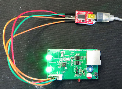
EPEVER to USB Converter

After reviewing the SoC datasheet, serial port settings of 115200, 8, N, 1 were used with a terminal program. The capture below shows the port settings for Tera Term.
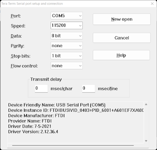
Tera Term Communications Settings for EPEVER Debug

WiFi Adaptor Output Log
The output log from the WiFi adaptor SoC shows that the RT-Thread RTOS is used. There is a plethora of reading material on the RT-Thread website including the
tools required for interfacing with the SoC. These software packages were not verified in this post.

In the log shown below, the default IP address of the WiFi adaptor is listed as 192.168.169.2 with a port of 65010 for communincations to the RS485 port.

[SFUD]Warning: Read SFDP parameter header information failed. The norflash is not support JEDEC SFDP.
[SFUD]Warning: This flash device is not found or not support.
[SFUD]Warning: Read SFDP parameter header information failed. The norflash is not support JEDEC SFDP.
[SFUD]Warning: This flash device is not found or not support.
[SFUD]Error: norflash flash device is initialize fail.
[I/FAL] RT-Thread Flash Abstraction Layer (V0.4.0) initialize success.
[E/OTA] (ota_main:41) download partition is not exist, please check your configuration!
[D/OTA] (ota_main:105) jump to APP!
redirect_addr:8010100, stk_addr:20005888, len:851968

 \ | /
- RT -     Thread Operating System
 / | \     4.0.2 build Feb 25 2022
 2006 - 2019 Copyright by rt-thread team
lwIP-2.0.2 initialized!
ERROR: SPI device fl_spi not found!
[I/sal.skt] Socket Abstraction Layer initialize success.
[D/FAL] (fal_flash_init:61) Flash device |w60x_onchip | addr: 0x08000000 | len: 0x00100000 | blk_size: 0x00001000 |initialized finish.
ERROR: Flash device w25q128 not found!
[D/FAL] (fal_flash_init:61) Flash device |norflash | addr: 0x00000000 | len: 0x00000000 | blk_size: 0x00000000 |initialized finish.
[D/FAL] (fal_partition_init:176) Find the partition table on 'w60x_onchip' offse                                     t @0x0000ff88.
[I/FAL] ==================== FAL partition table ====================
[I/FAL] | name       | flash_dev   |   offset   |    length  |
[I/FAL] -------------------------------------------------------------
[I/FAL] | app        | w60x_onchip | 0x00010100 | 0x000d0000 |
[I/FAL] | easyflash  | w60x_onchip | 0x000e0100 | 0x00004000 |
[I/FAL] | filesystem | w60x_onchip | 0x000e4100 | 0x00019000 |
[I/FAL] =============================================================
[I/FAL] RT-Thread Flash Abstraction Layer (V0.3.0) initialize success.
[Flash] (packages\EasyFlash-v3.3.0\src\ef_env.c:152) ENV start address is 0x00000000, size is 8192 bytes.
[Flash] (packages\EasyFlash-v3.3.0\src\ef_env.c:821) Calculate ENV CRC32 number is 0xD6114A34.
[Flash] (packages\EasyFlash-v3.3.0\src\ef_env.c:833) Verify ENV CRC32 result is OK.
[Flash] (packages\EasyFlash-v3.3.0\src\ef_env.c:821) Calculate ENV CRC32 number is 0x78CA81B2.
[Flash] (packages\EasyFlash-v3.3.0\src\ef_env.c:833) Verify ENV CRC32 result is OK.
[Flash] EasyFlash V3.3.0 is initialize success.
[Flash] You can get the latest version on https://github.com/armink/EasyFlash .
<--------------------software: GT100WS142W600T------------------>
tls_fls_init() return 2
init MyFile obj is success.
enter InitHnjdClass() success.
ql_dev_init()=0

<-- lt_sock_para_1()  APP_NV_SYS=,ret=0. ID=00065689.MAC=202205111459122 -->
<--init0 hnjd paraments success  loraSize=0-->
Hnjd_GetImei(), imei:202205111459122;
<--init hnjd paraments success  loraSize=0-->
init gpio class success.
RT-Thread create eventUart2Recv successful
init serial class success.
init logs class success.
Hnjd_GetImei(), imei:202205111459122;
SecCount=-1,SendCount=0
COM<-- 89 D2 D4 D2 D2 D4 CF D3 D3 D3 D0 CF CB D3 D2 D2 00 D4 D4 D4 D4 D4 D4 23 1D A8 88
msh />gpio task running......
serial task2 running......
COM--> 89 D2 D4 D2 D2 D4 CF D3 D3 D3 D0 CF CB D3 D2 D2 00 D2 D4 D4 CC D4 D3 23 1D 9D 88
TEA success.
init system success.
[D/DFS] enter AP mode

[I/WLAN.dev] wlan init success
[I/WLAN.lwip] eth device init ok name:w0
[I/WLAN.mgnt] start ap successs!
[D/DFS] rt_wlan_start_ap(HN_65689,12345678) return RT_EOK.

[D/DFS] main() enter UserMain()

enter InitSockClass()
exit InitSockClass()
[DHCP] dhcpd_start: w0
[DHCP] ip_start: [192.168.169.2]
[DHCP] ip_start: [192.168.169.254]
enter lt_RtuTask()
local ip:0.0.0.0 port:65010

TCPServer Waiting for client on port 65010...
RT-Thread create eventSockSendRecv successful
serial init success. baud=115200,parity=8N1


Should anyone want to delve further, typing help in Tera Term indicated the menus displayed below.

RT-Thread shell commands:
setenv           - Set an envrionment variable.
printenv         - Print all envrionment variables.
saveenv          - Save all envrionment variables to flash.
getvalue         - Get an envrionment variable by name.
resetenv         - Reset all envrionment variable to default.
fal              - FAL (Flash Abstraction Layer) operate.
ntp_sync         - Update time by NTP(Network Time Protocol): ntp_sync [host_name]
list_fd          - list file descriptor
date             - get date and time or set [year month day hour min sec]
sf               - SPI Flash operate.
wifi             - wifi command.
version          - show RT-Thread version information
list_thread      - list thread
list_sem         - list semaphore in system
list_event       - list event in system
list_mutex       - list mutex in system
list_mailbox     - list mail box in system
list_msgqueue    - list message queue in system
list_memheap     - list memory heap in system
list_mempool     - list memory pool in system
list_timer       - list timer in system
list_device      - list device in system
help             - RT-Thread shell help.
ls               - List information about the FILEs.
cp               - Copy SOURCE to DEST.
mv               - Rename SOURCE to DEST.
cat              - Concatenate FILE(s)
rm               - Remove(unlink) the FILE(s).
cd               - Change the shell working directory.
pwd              - Print the name of the current working directory.
mkdir            - Create the DIRECTORY.
mkfs             - format disk with file system
df               - disk free
echo             - echo string to file
ps               - List threads in the system.
time             - Execute command with time.
free             - Show the memory usage in the system.
ifconfig         - list the information of all network interfaces
ping             - ping network host
dns              - list and set the information of dns
netstat          - list the information of TCP / IP
smartconfig_demo - smartconfig demo
reboot           - Reboot System

msh />


To verify the WiFi adaptor was operating, a computer with a suitably configured WiFi IP address was tested with Putty.
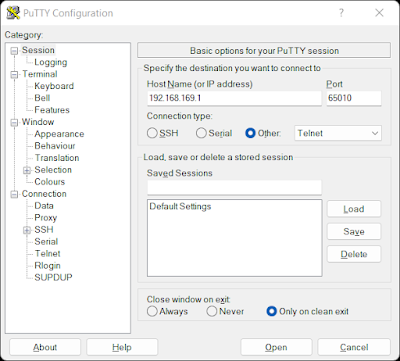
Putty Communications Settings for EPEVER Testing

With the Tera Term debug connection to the WiFi adaptor active, a connection using Putty was established. The packet highlighted in the capture below was received by the WiFi adaptor and appeared consistent with a connection from Putty.

[I/WLAN.mgnt] sta associated mac:bc:09:1b:eb:06:3b
I got a connection from (192.168.169.2 , 51147)
COM<-- FF FB 1F FF FB 20 FF FB 18 FF FB 27 FF FD 01 FF FB 03 FF FD 03


Final Thoughts
The test mentioned in this blog using Putty confirmed that the EPEVER WiFi adaptor worked. A separate test with an Android phone (point-to-point), not mentioned in this blog, did not show the same behaviour.

The access point connection with point-to-point or cloud is not a preferred solution. The WiFi adaptor firmware could likely be reconfigured to operate in station mode. Whether EPEVER is required to rebuild the source, or this option is already provided in the CLI remains to be determined. Station mode is supported by RT-Thread as indicated in the capture below.


[*] Using Wi-Fi framework                /* Using Wi-Fi framework */
(wlan0) The WiFi device name for station /* The default name for station */
(wlan1) The WiFi device name for ap      /* The default name for ap */
(lwip) Default transport protocol        /* Default protocol */
(10000) Set scan timeout time(ms)        /* Scan timeout time */
(10000) Set connect timeout time(ms)     /* Connect timeout time */
(32)  SSID name maximum length           /* Maximum length of SSID name */
(32)  Maximum password length            /* Maximum length of password */
[*]   Automatic sorting of scan results  /* Automatic sorting of scan results */
(3)   Maximum number of WiFi information automatically saved /* Maximum number of WiFi information automatically saved */
(wlan_job) WiFi work queue thread name   /* WiFi work queue thread name */
(2048) wifi work queue thread size       /* wifi work queue thread size */
(22)  WiFi work queue thread priority    /* WiFi work queue thread priority */
(2)   Maximum number of driver events    /* Maximum number of driver events in dev layer */
[ ]   Forced use of PBUF transmission    /* Forced use of PBUF transmission */
[ ]   Enable WLAN Debugging Options      /* Enable WLAN Debugging Options */


Monday, 26 September 2022

Salvaging Billion BiPAC 7700N

Introduction
This
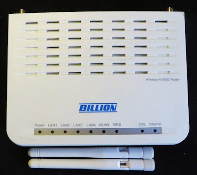
blog illustrates portions of hardware that can be salvaged from a Billion ADSL model BiPAC 7700N R2.

Billion BiPAC 7700N R2 ADSL Modem
 
Salvaging
The Billion model 7700N contained two user-fitted external antennas and an AC wall adaptor DC 12 V 1A. Due to the age of the antennas, the plastic around the screw portion of the antenna was perishing. Reusing would be possible since the plastic on the connector does not affect functionality.

Billion ADSL Modem Antennas

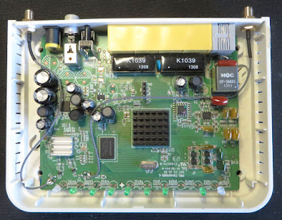
To access the internals of the modem, the four rubber feet on the bottom side of the model hide the plastic screws. Removing these allows access to the circuit board. For anyone with a 3D printer or repair cafe, the four plastic screws could be of use.

Billion BiPAC 7700N Internals

Two gold-plated SMA connectors can be salvaged however these are chassis mount and may not suit all designs.

Billion BiPAC 7700N Circuit Board

The two small aluminium heatsinks were easily pried off the Broadcom chips. Either the smaller silver-coloured heatsink (11 mm x 11 mm) or the larger black-coloured heatsink (20 mm x 20 mm) could be repurposed on other designs or single-board computers such as the Raspberry Pi.

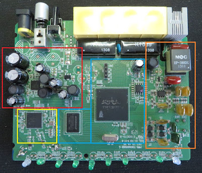
Billion BiPAC 7700N Circuit Board (ID Blocks)

The summary below relates to the components in the areas identified by the coloured boxes in the above image.

Red Box
The power supply uses a Texas Instruments triple output buck converter, TPS65251. The internal MOSFET resistances are suitable for a project; the overall efficiency is quite reasonable.

The passives surrounding the buck converter device are the support capacitors (EFC) and inductors. These parts could be salvaged if needed.

The associated right-angle PCB mount DC power jack and push-button power switch could be salvaged. It is presumed that the number of DC jack mating cycles and push-button switch actuations was minimal therefore repurposing would carry low risk.

Yellow Box
The Wi-Fi interfacing was managed by the Broadcom BCM43225 chip; likely not worth salvaging. Providing the clock for the Wi-Fi chip is an external 20 MHz crystal, worth removing as this is a standard 4-pin device.

Blue Boxes
The main CPU is a Broadcom BCM63281TK; likely not worth salvaging. Both the Macronix MX25L6445E serial flash and Winbond 256 Mb DDR2 DRAM W9725G6KB-25 may be useable devices. The external HC49S 20 MHZ crystal could be removed.

Orange Box
ADSL communications are handled by the Broadcom ADSL driver 6301KSG; only worth salvaging if required for repair or other projects. The associated ADSL line components, such as the line transformer and capacitors (100 V) would be worth salvaging for related projects or repairs.

Sundry Items
The remaining RJ-styled connectors and leaded LEDs could be salvaged for other projects.

Billion BiPAC 7700N Circuit Board Bottom Side

Flipping the circuit board over shows the reset switch and the obligatory passives such as inductors and decoupling capacitors. These passive components are not usually worth salvaging however as with any hardware salvage, the devices are based on the requirement.

Tornado Cleaning Brush Circuit

Introduction
This
micro-blog presents the electronics circuit and motor part number details for a well-known battery-powered cleaning brush.

Electronics
The product design consists of a DC motor, rechargeable battery and associated battery charge monitor. Provided with the product is an external mains power adaptor as the recharging source.

DC Motor from Cleaning Brush

The motor is rated at DC 3.6 V, part number RS390SH-6213. A similar motor can be sourced at companies such as AliExpress.

Powering the motor during the use of the cleaner is a standard Li-Ion battery (18650) with a rating of 3.7 V 2.2 AH.

Monitoring the charge state of the Li_Ion battery is an unidentified chip. The part number on the 8-pin chip (SOIC-8) was removed by linishing or a similar process.

Top Side of Cleaning Brush Circuit Board

Bottom Side of Cleaning Brush Circuit Board

The circuit containing the unidentified chip is displayed below.

Cleaning Brush Circuit

Sunday, 28 August 2022

Paralleling Outputs of High Side MOSFET Drivers

Introduction
This
blog measures the voltage and timing differences during simultaneous control of dual output high-side electronic drivers.

Parallel Dual High-Side Driver Test PCB

Test Device
The electronic component discussed in this blog is the IPS2050H. This device is manufactured by ST Micro. The device is a dual output high-side driver with an operating voltage of DC 8 – 60 V with a current capability of either 2.4 A or 5.6 A.

This ST driver was originally considered for the Interruption Tester project which is detailed in another series of posts. Paralleling the outputs of the IPS2050H for a higher current remained a matter of interest however several characteristics of these devices are not listed in the datasheet. Information such as the difference between channel ON/OFF control voltages or switching times was seen as beneficial.

Paralleling Outputs
Literature
on the subject of balancing currents when paralleling discrete MOSFETs is widely available. One such paper, “Paralleling of Power MOSFETs for HigherPower Output”, by James B. Forsythe of International Rectifier, provides a well-documented explanation of effects and techniques to normalise current sharing between MOSFET devices. In this post, some of the points listed in the International Rectifier paper were discussed and applied to the IPS2050H.

For further reading, Texas Instruments has a similar document "High Side Switches Paralleling Channels"

In a document with similar content, Infineon published an application note showing realistic gate voltage for high current applications "Paralleling MOSFETs in high-current LV drive applications"

Discussion
For those readers looking for an immediate answer to paralleling outputs of high-side drivers with multiple outputs, it is possible however the operation depends on the requirements of the load and driver.

The International Rectifier paper for MOSFETs was used as a guideline to review some aspects of the IPS2050H. Items from Section IV (c) Summary of Recommendations for Balancing Parallel MOSFET Currents were applied where possible.

Manufacturing of the IPS2050H would likely be performed on a single silicon wafer however there is commonly variation in characteristics across the wafer. Screening and parameter matching for the IPS2050H are not practical however, measurements were performed to determine differences between the devices two channels.

Parameter differences between channels were noted for Vin (ON) and (OFF).

IPS2050H Measured ON-OFF Voltages

The delays between input and output switching were measured at room  temperature, approximately 1.96 us for both channels.

IPS2050H Input to Output Switching Delay (No Load)

The measurement for the switching delay was performed based on the
50 % input voltage and 10 % output voltage for the propagation delay as shown in Figure 3 of the IPS2050H datasheet.

Figure 3 Timing from IPS2050 Datasheet (Courtesy ST Micro)

When switching the input of both channels ON simultaneously, without a load connected to either, the turn ON delay between channels was approximately 400 ns.

IPS2050H Turn-ON Delay between Outputs

Next, a load consisting of a 10 R wire wound resistor was added to each channel. The turn-ON delay with the resistor was 17 us for one channel and 18 us for the other. The turn-OFF delay with the wire wound resistor was slightly over 7 us for both channels.

IPS2050H Channel 1 Turn ON Delay with Wirewound Resistor
IPS2050H Channel 1 Turn-ON Delay with Wire Wound Resistor

IPS2050H Channel 2 Turn-ON Delay with Wire Wound Resistor

The output turn-ON delay between channel 1 and 2 with separate wire wound resistors was slightly over 25 us for both channels.

IPS2050H Channel 1 to 2 Output Turn-ON Delay with Wire Wound Resistors

The output turn-OFF delay between channel 1 and 2 with separate wire wound resistors was again slightly over 7 us for both channels.

IPS2050H Channel 1 to 2 Output Turn-OFF Delay with Wire Wound Resistors

A capacitive load of 6800 uf was driven with various output configurations. For the first test, the two outputs were connected in parallel and wired to the capacitor. The charging waveform is shown below.

IPS2050H Parallel Channel 1 to 2 Capacitor Charging

For the subsequent test, the two outputs each had a 3.3 R current sharing resistor fitted before terminating at the capacitor. As expected the capacitor charge time constant increased because of the introduced resistance.

IPS2050H Parallel Channel 1 to 2 Capacitor Charging through 3.3 R Resistors

In the last configuration, two Schottky diodes were fitted to replace the resistors on each output before connecting to the capacitor.

IPS2050H Parallel Channel 1 to 2 Capacitor Charging through Schottky Diodes

The time to charge the capacitor with Schottky diodes was approximately the same as the directly connected paralleled outputs. Note the lower voltage across the capacitor with the diodes due to forward voltage losses.

Each channel of the IPS2050H driver was individually loaded to 1.5 A and the voltage across separate wire wound resistors was measured with both inputs of the device ON. The output voltage at channel 1 measured 15.051 V and channel 2 measured 15.089 V.

The IPS2050H inputs were driven using a square wave with a 90 % duty cycle. The output voltage at channel 1 measured 14.968 V and channel 2 measured 15.015 V.

Driving IPS2050H Channel 1 and 2 with a Square Wave

PCB Traces
As stated in the paper by
International Rectifier, the addition of series resistance would not be required for a design with MOSFETs. The traces on the test PCB outputs were duplicated as shown in the image below.

Highlighted Output Polygon Traces on Top Layer of Test PCB
 

Common source inductance was not reviewed in this post. Since the MOSFET gates are not accessible, drive modifications were not possible. The decoupling resistance (gate resistor) would likely be part of the control circuit block in the IPS2050H, as shown in the capture below, therefore this was also not investigated.

IPS2050H Functional Block Datasheet (Courtesy ST Micro)

Final Thoughts
Measurements performed on the IPS2050H indicated there are
minor difference in turn ON/OFF threshold voltages and switching delays. These timing differences may result in one channel of the IPS2050H momentarily handling most of the switching energy at on turn ON and then at turn OFF. This time difference was measured in microseconds for the loads tested, which may be acceptable time for some designs but a hindrance for other designs where high instantaneous currents are required.

For a more comprehensive review, current measurements from each of the parallel outputs in a target circuit would provide clarity on the demand placed on each driver output. Temperature measurements could also prove beneficial to ensure that the device’s maximum operating specifications were not exceeded.

Friday, 15 July 2022

Voltage Interruption Tester for IEC 61496-1 Part 5

Introduction
This blog continues from part 4 and finalised the supply voltage interruption tester (unit) post. 

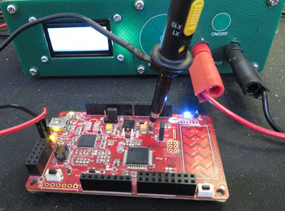
Covered in this blog is an interruption test applied to a PSoC development board. The test setup consisted of a Rigol DP832, the Interruption tester prototype and the PSoC development board part CY8CKIT-042.

Interruption Test Setup Using PSoC Development Board

This post also provides the source and Gerber files for the interruption tester project.

Practical Interruption Test

Disclaimer - The interruption test performed on the Cypress PSoC development board was performed for the sole purpose of measurement and testing only. The PSoC development board does not claim conformance with the test conducted.

Only interruption test 1 was performed because the operating voltage of the development board was stated as DC 5 – 12 V and the minimum operating voltage for the interruption tester output drivers is DC 8 V. Test 2 and 3 require half the supply voltage which was not practical.
For the program operating on the PSoC board, two outputs of a PWM block were used to separately toggle the onboard bi-colour LED.

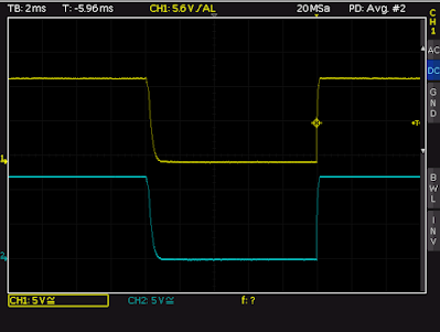
When interruption test 1 was enabled, the 3.3 V supply was interrupted which resulted in the processor resetting. This is evident by the irregular operation of the bi-colour LED.


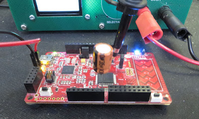
To resolve the issue caused by the dips in the supply rail, a 100 uF electrolytic capacitor was connected across the development board supply.


The two images below show a capture of the 3.3 V supply before and after the 100 uF capacitor was added to the development board.

Capture of Supply Rail During Interruption Test

Capture of Supply Rail During Interruption Test with Additional Capacitor

Shown in the image below is the location where the additional 100 uF capacitor was added to the development board.

Interruption Test Setup PSoC Development Board with Capacitor

While this test is straightforward on simple hardware, it shows the basic process behind interruption testing.

Final Comments
This series of blog posts focused on an overall view of the hardware design for the power supply interruption tester. While not every aspect of the design process was covered in detail, design files have been provided in the Downloads section to assist those interested in producing a similar project.

Downloads
Listed below are the PSoC Creator project, Gerber and BOM files for the Interruption Tester project. This project is supplied as shown in this blog (Posts 1 to 5).

Display Schematic and BOM

Display Gerber and NC Drill

Driver Schematic and BOM

Driver Gerber and NC Drill

Rear Panel Gerber and NC Drill

PSoC Creator Project (Complete Archived)


Wednesday, 13 July 2022

PSoC Silicon ID Header File Creation

Summary
This blog offers a solution to generate PSoC header files from Cypress DAT files using PowerShell scripts. Available Cypress DAT files are merged and then converted into a single header file.

There is a thread similar to this post on the Infineon website called ‘JTAG/Silicon ID reference file’.

History
Fluctuations in global chip levels have resulted in a wider range of microcontrollers seen by companies responsible for programming and testing electronic hardware. 

To accommodate changes in microcontrollers using a more automated process for creating software header files, the scripts mentioned in this blog were designed. These scripts are fully functional, however, not without limitations as this is an initial foray into splitting scripts with this type of file content manipulation. 

The scripts were written in two parts because one script was made to run in the Program Files directory that contains the relevant DAT files. The second script was made to run with the merged DAT file.

Installation Requirement
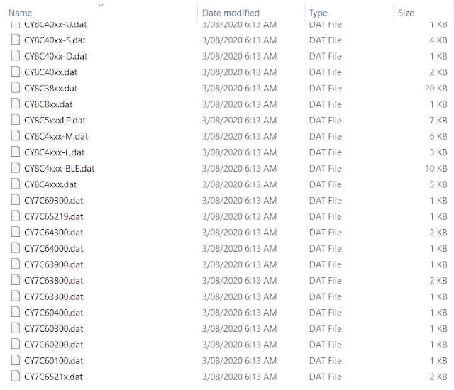
To access the DAT files, the Cypress (Infineon) PSoC Programmer should be installed. The DAT files are located at the following location - C:\Program Files (x86)\Cypress\Programmer\Devices

Example of Cypress .DAT File Listing

The DAT files contain various items of PSoC information. Of this, the device name and ID range are of primary interest. 

As an example for PSoC device CY8C4125AZI-473, the entry from file CY8C4xxx.dat is displayed below.

2,CY8C4125AZI-473, CY8C4125AZI-473, 48, 32768, 3, 04_2B_11_93, 04_2B_12_93, v33


Whether the PSoC ID is utilised to program PSoC devices or other information such as the size of the flash is needed for programming file verification, the PowerShell script could easily be adapted to suit these purposes.

Implementation
The first script called 'dat_merger.ps1' combines multiple DAT files using the PowerShell add-content command. The script was designed to handle all DAT files in the Cypress Programmer Devices directory however the script will also work on a single DAT file. 

Additionally, the first row in each DAT file is removed since this is redundant. To process the file in the next script, the merged file is saved in CSV format.

$dir = Get-Location
Write-Host "Merging Files"

$source ="$dir\*.dat"
$destination = "$dir\merge.csv"

# Remove first row and merge all files in directory
Get-ChildItem -Filter '*.dat' | ForEach-Object {
Get-Content $_ | Select -Skip 1 | Add-Content $destination
}


The second script dat_parser.ps1 removes any unwanted columns, selects only the first column of PSoC IDs, adds the text ‘#define’, formats the ID into a preferred value by stripping the formatting and then saves the result as a jtag.h file.

$dir = Get-Location
Write-Host "Parsing files in $dir"
# Grab merged csv files
$source = "$dir\merge.csv"
$destination ="$dir\jtag.h"

# Strip columns, add hash define and number format for each line, strip CSV then save as header file
Import-CSV-Delim ','$source -Header a,b, c, d, e, f, g |
Select "b","g" | ForEach-Object {$_."b" = "#define $($_."b")";$_} |
ForEach-Object {$_."g" = "0x$($_."g")";$_} |
ConvertTo-Csv -NoTypeInformation |
Select-Object -Skip 1 |
# Option for tab instead of spaces
#% { $_ -replace ‘_‘, “” -replace (‘,‘, "`t")  -replace ('"', '')} |
% { $_ -replace _‘, “” -replace (‘,‘, ''.padleft(10, ' '))  -replace ('"','')} |
Out-File $destination -Encoding utf8


Output
The first script would merge DAT files. Two example files were chosen CY8C42xx-D.dat and CY8C44xx.dat.

Before Script 

1,CY8C42xx-D, CY8C42xx-D, 8, 5, 128
2,CY8C4245PVI-DS402, CY8C4245PVI-DS402, 28, 32768, 3, 17_03_11_A7, v17
2,CY8C4245FNI-DS402, CY8C4245FNI-DS402, 25, 32768, 3, 17_02_11_A7, v17
2,CY8C4246PVI-DS402, CY8C4246PVI-DS402, 28, 65536, 3, 17_01_11_A7, v17
2,CY8C4246FNI-DS402, CY8C4246FNI-DS402, 25, 65536, 3, 17_00_11_A7, v17

1,CY8C44xx, CY8C44xx, 8, 5, 128
2,CY8C4A45PVI-481, CY8C4A45PVI-481, 28, 32768, 3, 1C_02_11_AC, v17
2,CY8C4A45FNI-483, CY8C4A45FNI-483, 45, 32768, 3, 1C_03_11_AC, v17
2,CY8C4A45LQI-483, CY8C4A45LQI-483, 48, 32768, 3, 1C_00_11_AC, v17
2,CY8C4A45AZI-483, CY8C4A45AZI-483, 48, 32768, 3, 1C_01_11_AC, v17
2,CY8C4A45FNQ-483, CY8C4A45FNQ-483, 45, 32768, 3, 1C_41_11_AC, v17
2,CY8C4A45LQQ-483, CY8C4A45LQQ-483, 48, 32768, 3, 1C_40_11_AC, v17

After Script 
2,CY8C4245PVI-DS402, CY8C4245PVI-DS402, 28, 32768, 3, 17_03_11_A7, v17
2,CY8C4245FNI-DS402, CY8C4245FNI-DS402, 25, 32768, 3, 17_02_11_A7, v17
2,CY8C4246PVI-DS402, CY8C4246PVI-DS402, 28, 65536, 3, 17_01_11_A7, v17
2,CY8C4246FNI-DS402, CY8C4246FNI-DS402, 25, 65536, 3, 17_00_11_A7, v17
2,CY8C4A45PVI-481, CY8C4A45PVI-481, 28, 32768, 3, 1C_02_11_AC, v17
2,CY8C4A45FNI-483, CY8C4A45FNI-483, 45, 32768, 3, 1C_03_11_AC, v17
2,CY8C4A45LQI-483, CY8C4A45LQI-483, 48, 32768, 3, 1C_00_11_AC, v17
2,CY8C4A45AZI-483, CY8C4A45AZI-483, 48, 32768, 3, 1C_01_11_AC, v17
2,CY8C4A45FNQ-483, CY8C4A45FNQ-483, 45, 32768, 3, 1C_41_11_AC, v17
2,CY8C4A45LQQ-483, CY8C4A45LQQ-483, 48, 32768, 3, 1C_40_11_AC, v17


Running the second script on the merged file output from the first script results in a new file called jtag.h as shown below.

#define CY8C4245PVI-DS402         0x170311A7
#define CY8C4245FNI-DS402         0x170211A7
#define CY8C4246PVI-DS402         0x170111A7
#define CY8C4246FNI-DS402         0x170011A7
#define CY8C4A45PVI-481         0x1C0211AC
#define CY8C4A45FNI-483         0x1C0311AC
#define CY8C4A45LQI-483         0x1C0011AC
#define CY8C4A45AZI-483         0x1C0111AC
#define CY8C4A45FNQ-483         0x1C4111AC
#define CY8C4A45LQQ-483         0x1C4011AC

One of the limitations with the current implementation is the uneven padding between the PSoC device name and the ID. The parser code inserts ten white spaces which may not conform with all programming styles.

Final Thoughts
The PowerShell scripts (under GPL) have been tested on several DAT files however the outputs should be verified as part of standard practice. Improvements are welcomed!

Downloads
 

Cypress Dat Merger PowerShell Script
dat_merger.ps1

Cypress Dat Merger PowerShell Script
dat_parser.ps1

Cypress Dat Merger PowerShell Script
jtag.h
(Example of PSoC4, PSoC5)